
LCD device

A liquid crystal display device and pixel technology, which is applied in static indicators, nonlinear optics, instruments, etc., can solve the problems of flicker and uneven picture of the liquid crystal display device.

Inactive Publication Date: 2008-12-10
INNOLUX CORP
View PDF0 Cites 19 Cited by
  • Summary
  • Abstract
  • Description
  • Claims
  • Application Information

AI Technical Summary

Problems solved by technology

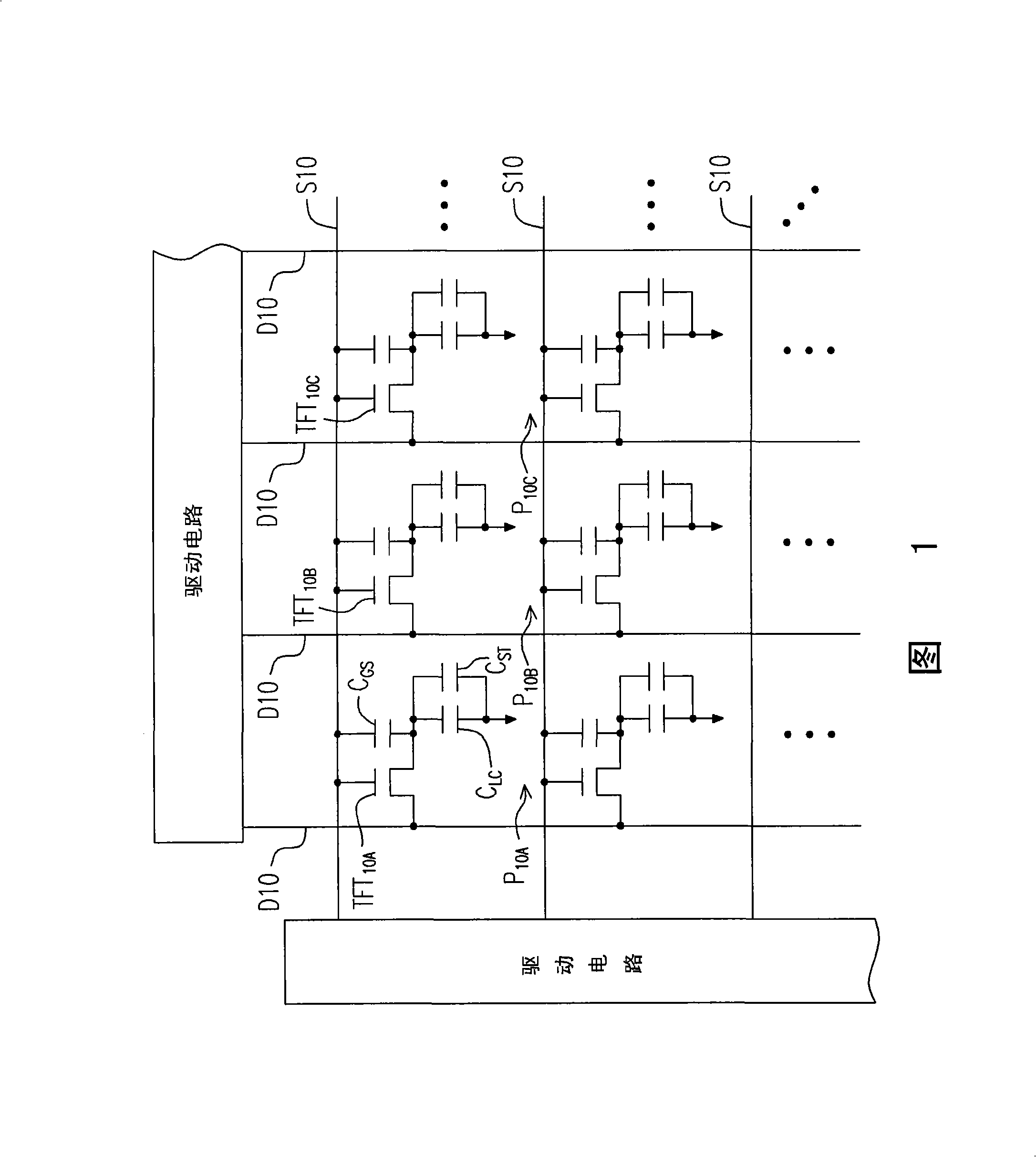
However, (V gh -V gl ) will become smaller as the distance between the pixel and the input terminal of the scanning wiring is farther away, that is, the pixel P shown in Figure 1 10A ,P 10B ,P 10C (V gh -V gl ) will render (V gh -V gl ) 10A >(V gh -V gl ) 10B >(V gh -V gl ) 10C The phenomenon
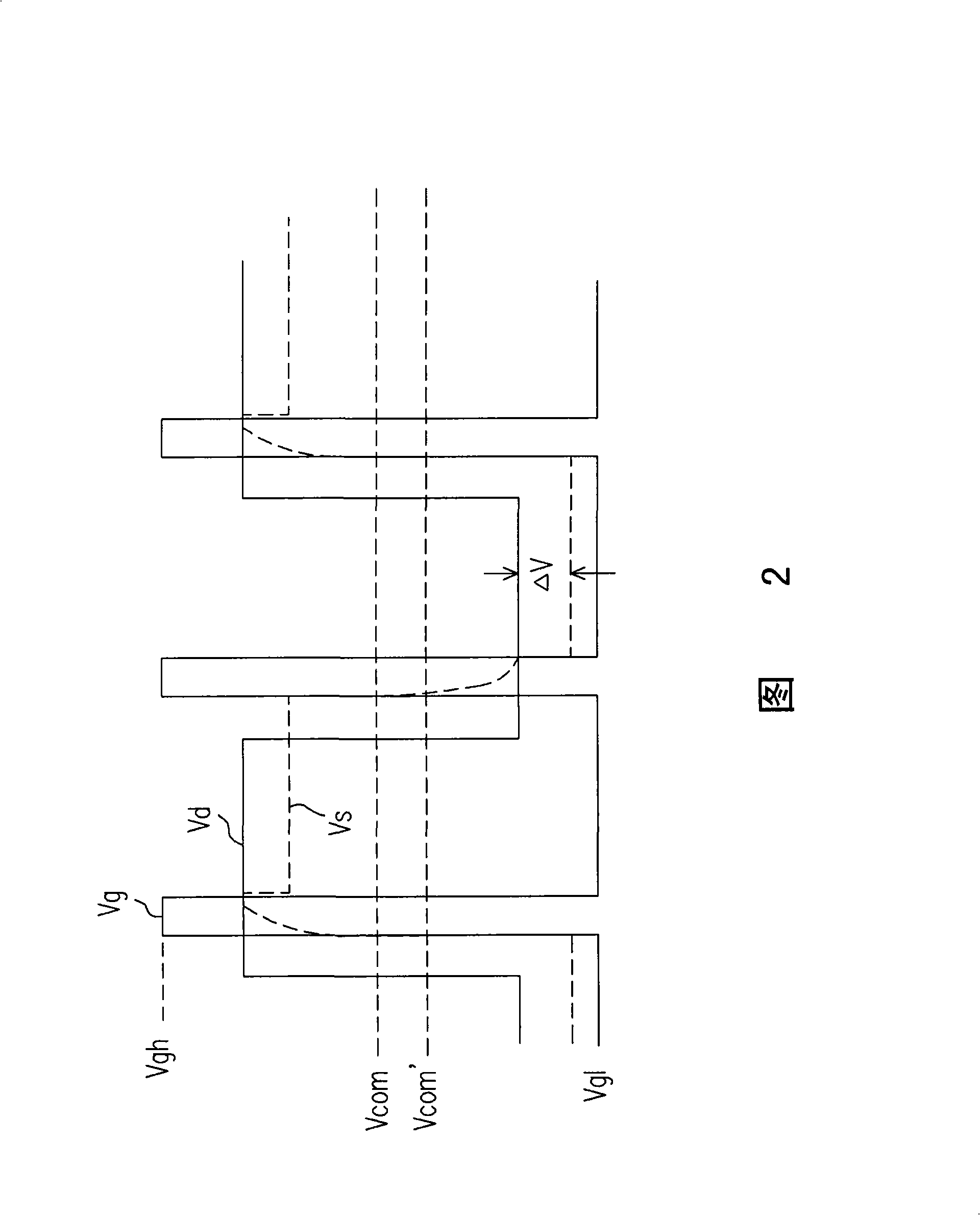
Therefore, according to equation (1), when the C of each pixel LC 、C ST 、C GS are the same, the pixel P 10A ,P 10B ,P 10C The feedthrough voltage ΔV will present ΔV 10A >ΔV 10B >ΔV 10C However, there is still an uneven feed-through voltage ΔV, which makes the screen of the liquid crystal display device uneven and flickering.

Method used


Image

  • LCD device
  • LCD device
  • LCD device

Examples


Embodiment Construction

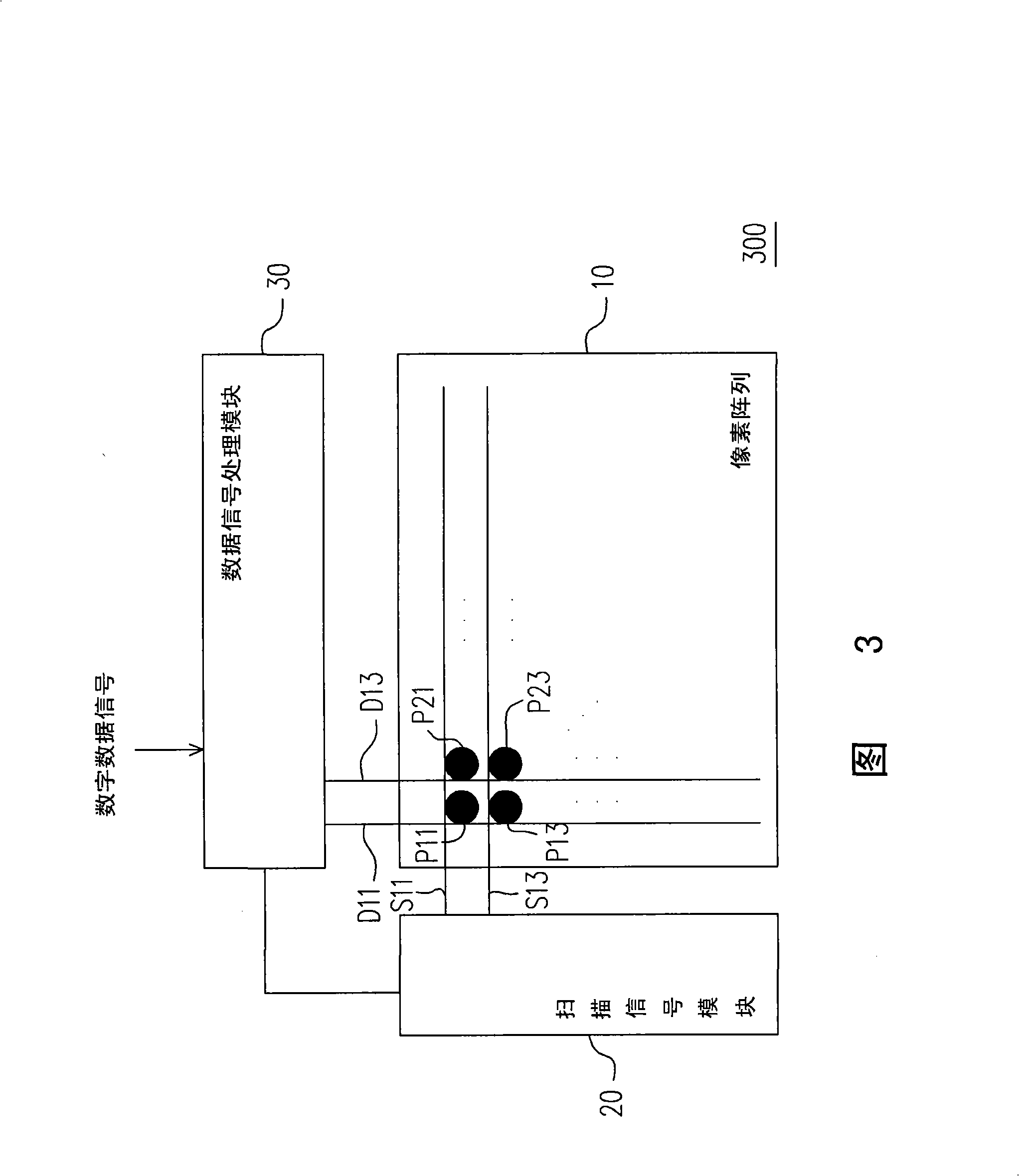
[0060] FIG. 3 is a schematic diagram of a liquid crystal display device according to a first embodiment of the present invention. Please refer to FIG. 3 , a liquid crystal display device 300 includes a pixel array 10, a plurality of scanning lines (indicated by scanning lines S11 and S13), a plurality of data lines (indicated by data lines D11 and D13), a scanning signal module 20 and data signal processing Module 30. The pixel array 10 includes a plurality of pixels (represented by pixels P11 , P13 , P21 and P23 ). In this embodiment, the number of scan lines, the number of data lines and the number of pixels are described as two, two, and four, respectively. Those skilled in the art should know that the "number of scan lines", "number of data lines" and "number of pixels" mentioned in this embodiment are only a specific embodiment. In other embodiments, the "number of scan lines" , "number of data lines" and "number of pixels" can be other numbers, so the present invention...


PUM


Abstract

The present invention discloses a liquid crystal display device which comprises a pixel array, a plurality of scanning beams, a plurality of data wires, a scanning signal module and a data signal processing module; wherein, the pixel array comprises a plurality of pixels; the scanning signal module conveys scanning signals to the pixels by scanning beams; the data signal processing module is coupled with the data wires for compensating and transforming received data signals to produce simulative voltage signals and for compensating positive voltage to the simulative voltage signals which are conveyed to the pixels through the data wires. The positive voltage compensation is reduced as the distance between each pixel and the input ends of the scanning wires is increased, so the problem of the uneven picture is solved.

Description

technical field [0001] The present invention relates to a liquid crystal display device (Liquid Crystal Display, LCD), and more particularly to a liquid crystal display device capable of preventing image mura. Background technique [0002] The rapid progress of the multimedia society is mostly due to the rapid progress of semiconductor components or man-machine display devices. As far as display devices are concerned, flat panel display devices with superior characteristics such as high image quality, good space utilization efficiency, low power consumption, and no radiation have gradually become the mainstream of the market. Among various flat display devices, thin film transistor (Thin Film Transistor, TFT) liquid crystal display devices are currently the most mature flat display devices. [0003] FIG. 1 is a schematic circuit diagram of a conventional thin film transistor liquid crystal display device. Please refer to Figure 1, the pixels P on the same row of a general ...

Claims


Application Information

Patent Timeline
Patent Type & Authority Applications(China)
IPC IPC(8): G02F1/1362G02F1/133G09G3/36
Inventor 纪佳宏蔡永裕
Owner INNOLUX CORP
Learn More