A/d conversion circuit, control method thereof, solid-state imaging device, and imaging apparatus

一种转换电路、电压的技术,应用在模数转换器、模/数转换、代码转换等方向,能够解决难以同时实现电路部分小面积占用和噪声减少等问题,达到减少占用面积的效果

Inactive Publication Date: 2008-12-10
SONY CORP
View PDF1 Cites 33 Cited by
  • Summary
  • Abstract
  • Description
  • Claims
  • Application Information

AI Technical Summary

Problems solved by technology

[0002] In a solid-state imaging device such as CMOS (Complementary Metal Oxide Semiconductor), it may be difficult to simultaneously achieve small area occupation of the circuit part and noise reduction

Method used


Image

  • A/d conversion circuit, control method thereof, solid-state imaging device, and imaging apparatus
  • A/d conversion circuit, control method thereof, solid-state imaging device, and imaging apparatus
  • A/d conversion circuit, control method thereof, solid-state imaging device, and imaging apparatus

Examples


Embodiment Construction

[0022] Hereinafter, embodiments of the present invention will be described in detail with reference to the accompanying drawings.

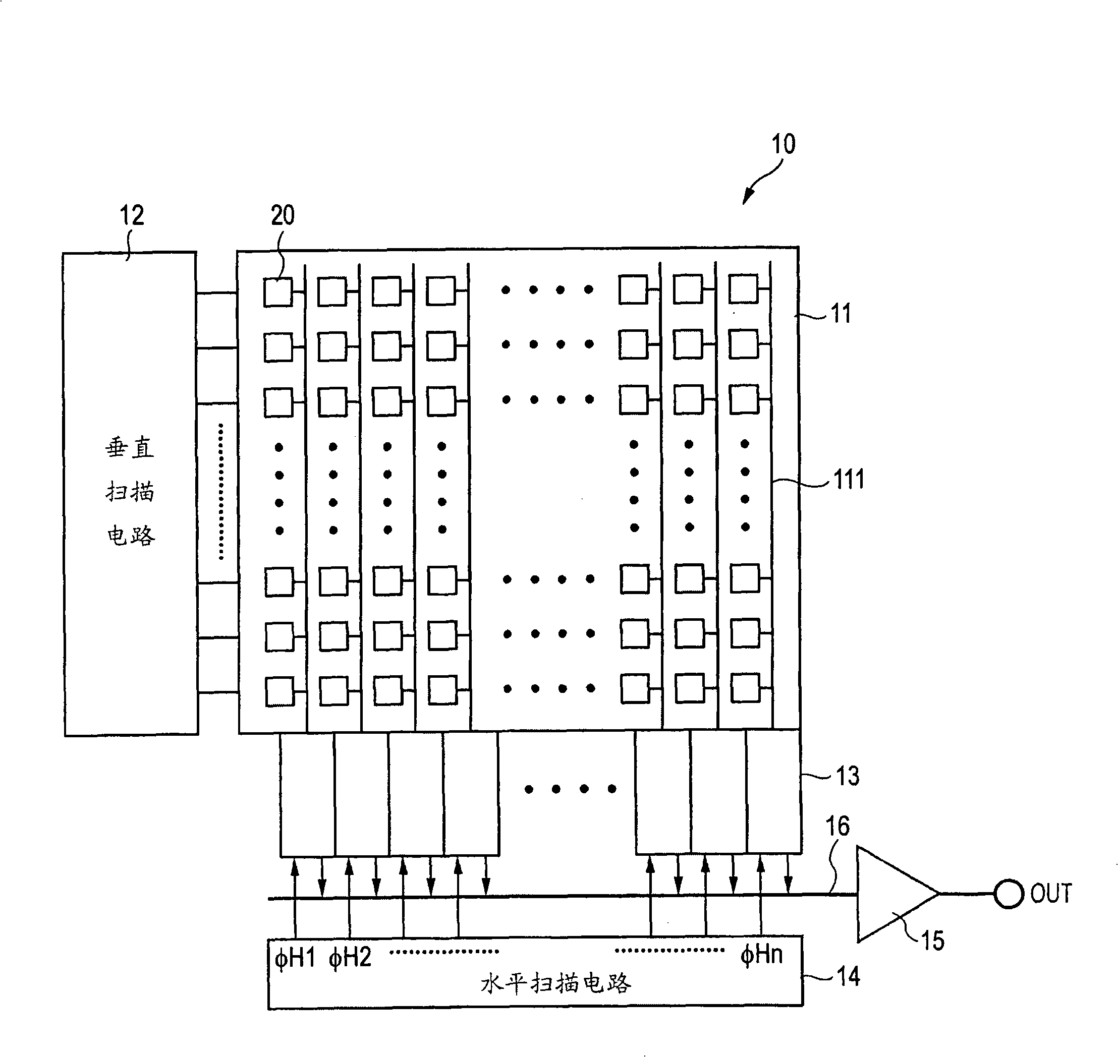
[0023] figure 1 is a system configuration diagram showing an example of a solid-state imaging element such as a CMOS image sensor to which the present invention is applied.

[0024] Such as figure 1 As shown, the CMOS imaging sensor 10 according to the embodiment includes: a pixel array section 11 in which unit pixels (hereinafter, also simply referred to as "pixels") each having a photoelectric conversion element are arranged in a matrix and in a two-dimensional manner 20; and peripheral circuits.

[0025] The peripheral circuits of the pixel array section 11 include, for example, a vertical scanning circuit 12, a column circuit 13, a horizontal scanning circuit 14, an output circuit 15, and the like. These circuits are integrated on the same chip (semiconductor substrate) as the pixel array section 11 .

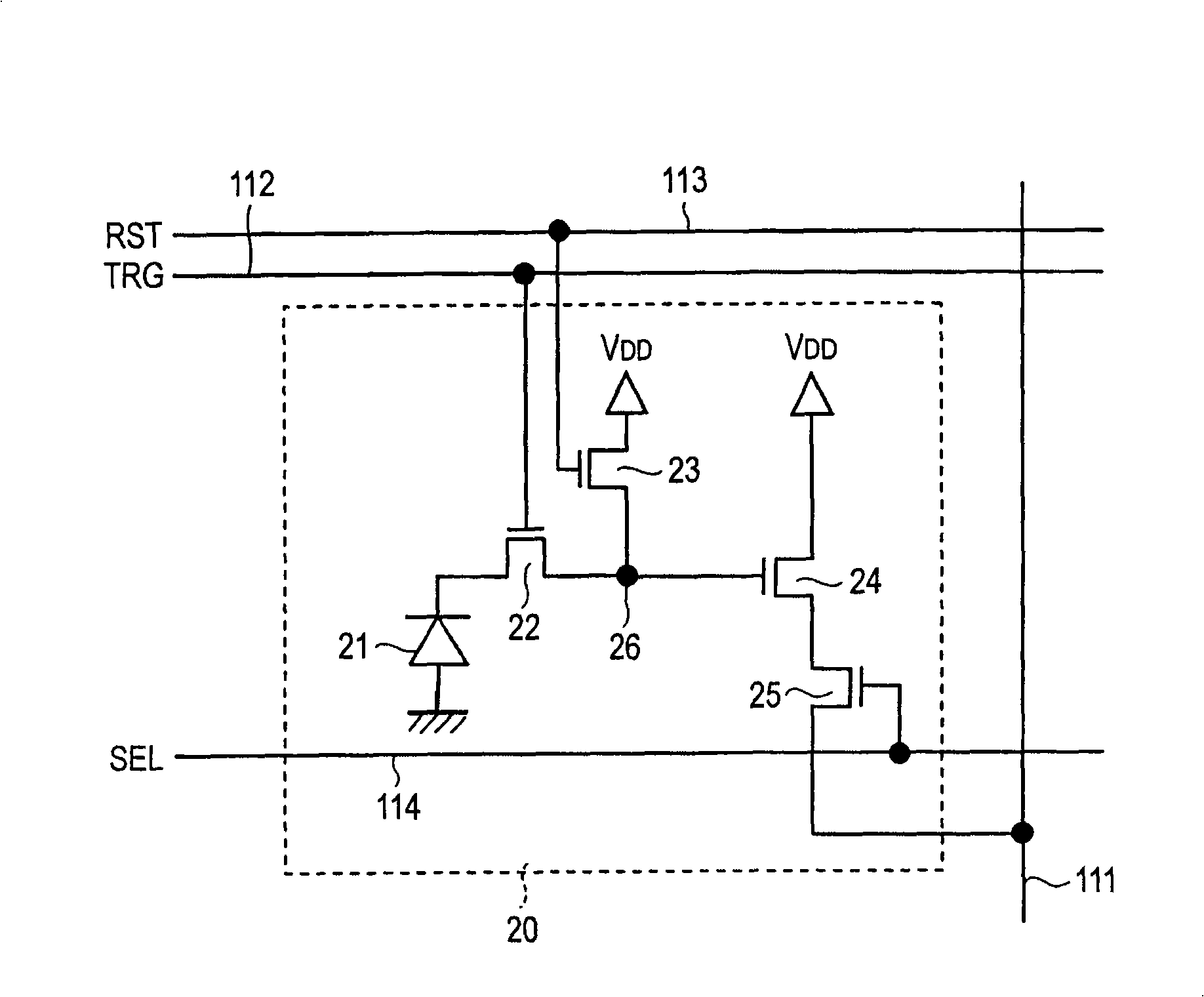
[0026] In the matrix arrangement of ...


PUM


Abstract

An A / D conversion circuit includes: an input capacitance to which an input signal and a reference signal are sequentially applied; an operational amplifier; a first switch connected between the other end of the input capacitance and a first input end of the operational amplifier; a feedback capacitance connected to the first input end of the operational amplifier; a second switch connected between the other end of the feedback capacitance and an output end of the operational amplifier; a third switch selectively applying a predetermined voltage to the other end of the feedback capacitance; a fourth switch selectively causing a short circuit between the first input end and the output end of the operational amplifier; a fifth switch applying the predetermined voltage to a second input end of the operational amplifier; and a sixth switch applying a ramp reference voltage to the second input end of the operational amplifier.

Description

technical field [0001] The present invention relates to an analog-digital (A / D) conversion circuit and a control method thereof, a solid-state imaging device, and an imaging device. Specifically, the present invention relates to an A / D conversion circuit having a comparator and a control method thereof, a solid-state imaging device using the A / D conversion circuit, and an imaging apparatus having the solid-state imaging device. Background technique [0002] In a solid-state imaging device such as a CMOS (Complementary Metal Oxide Semiconductor), it may be difficult to simultaneously achieve small area occupation of a circuit portion and noise reduction. In order to reduce noise in a CMOS image sensor, there is known a technique in which a readout circuit (column circuit) is arranged for each column in which pixels of a pixel array section are arranged to read out from a pixel To read out a signal, this technique amplifies the signal by performing arithmetic on a narrow nois...

Claims


Application Information

Patent Timeline
Patent Type & Authority Applications(China)
IPC IPC(8): H03M1/34H04N3/15H04N5/335H04N5/357H04N5/374H04N5/378
CPCH03M1/0658H03M1/56H04N25/616H04N25/75H03M1/12
Inventor 榊原雅树
Owner SONY CORP
Why Eureka
Try Eureka