A large area organic diode device and a method of manufacturing it

A diode and organic technology, applied in the field of organic diode devices, can solve the problems of complex manufacturing, winding of electric leads, etc., and achieve the effect of improving electrical contact and long life

Inactive Publication Date: 2008-12-17
KONINKLIJKE PHILIPS ELECTRONICS NV
View PDF2 Cites 9 Cited by
  • Summary
  • Abstract
  • Description
  • Claims
  • Application Information

AI Technical Summary

Problems solved by technology

[0005] A problem with the OLED in US 2004 / 0121508 A1 is that it is complex to manufacture due to the isolated electrical leads with non-insulated end sections, which have to be connected to the metal grid by means of conductive glue
The large number of electrical leads wrapped around the OLED surface is also unattractive from an aesthetic point of view

Method used


Image

  • A large area organic diode device and a method of manufacturing it
  • A large area organic diode device and a method of manufacturing it
  • A large area organic diode device and a method of manufacturing it

Examples


Embodiment Construction

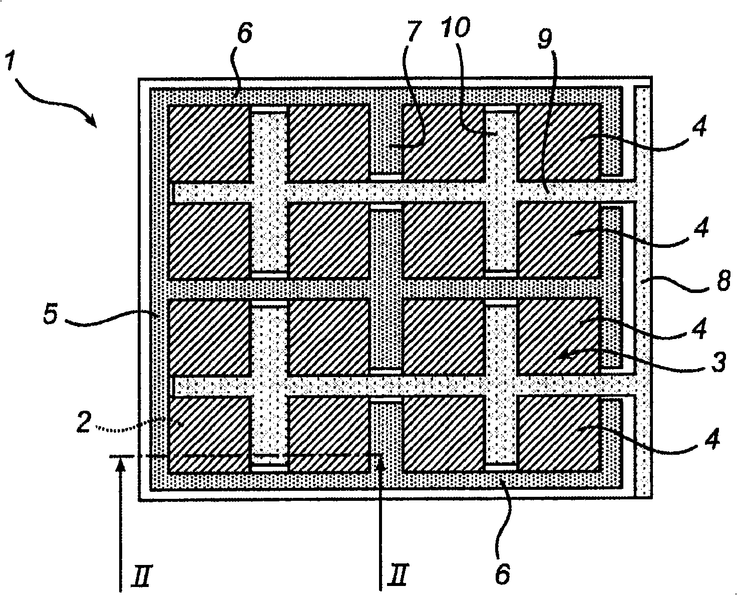
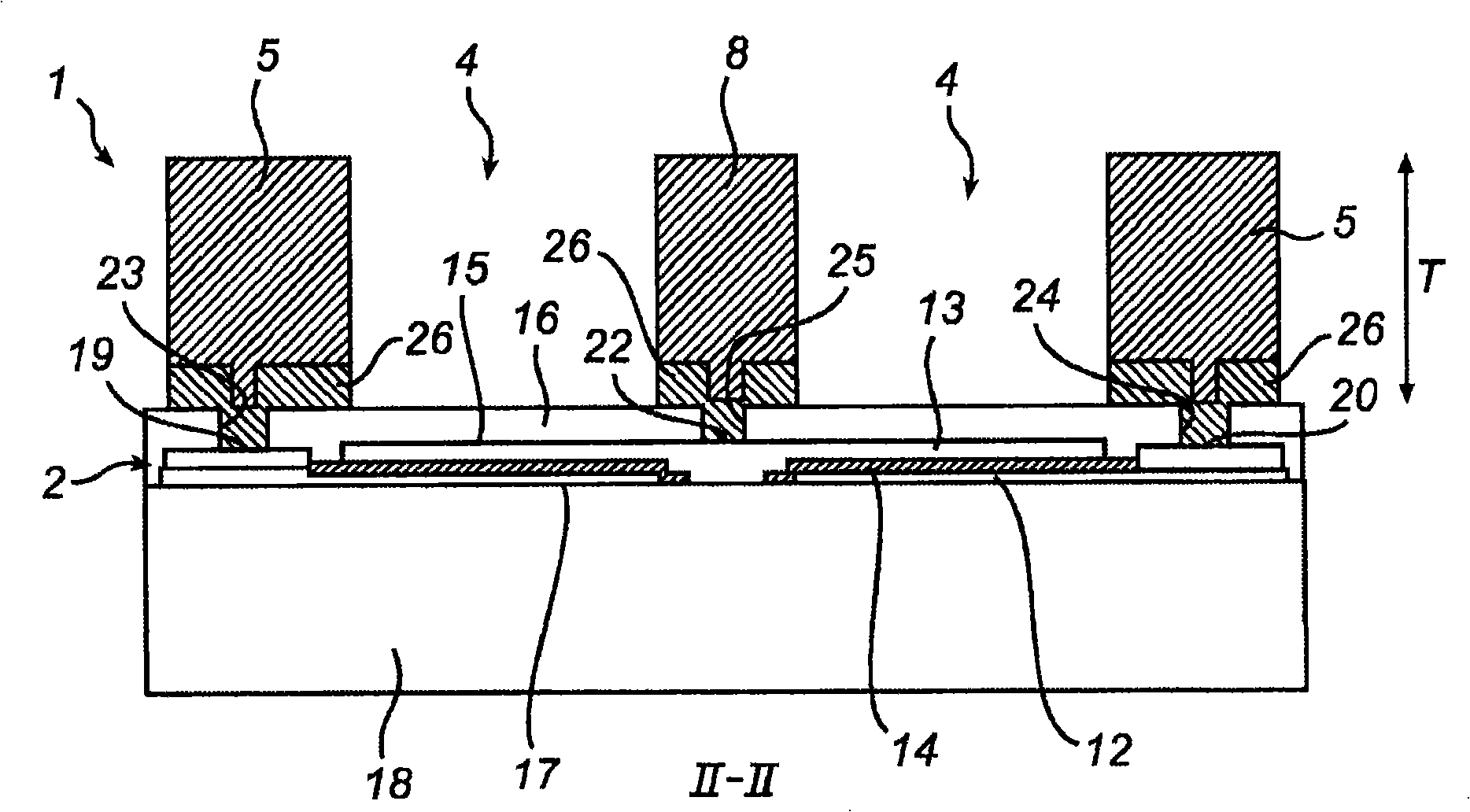
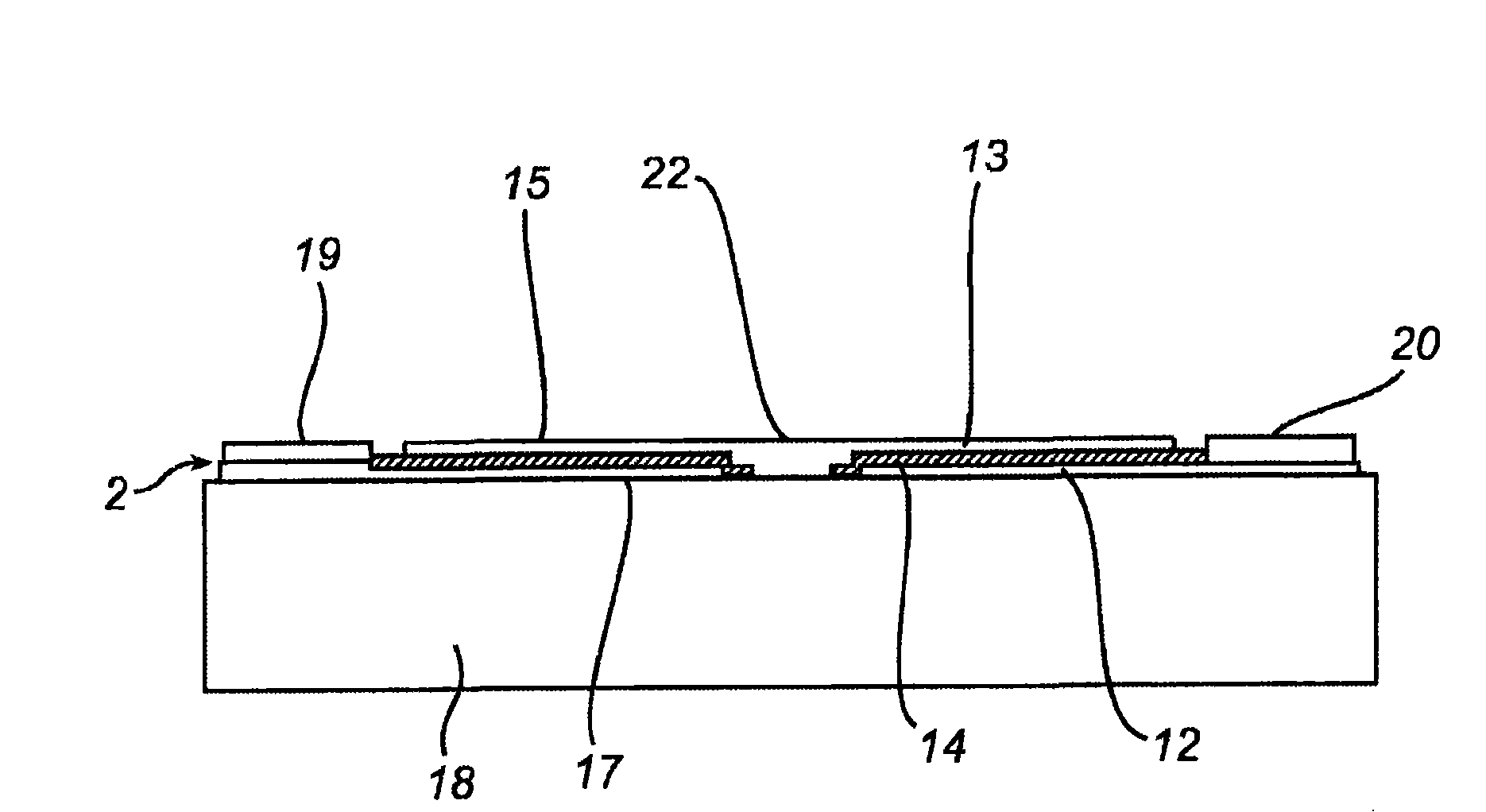
[0038] figure 1 An organic diode device in the form of a light emitting device 1 is shown. The light emitting device 1 comprises a light emitting structure 2, which is in figure 2 is shown in more detail. The light emitting device 1 has a large surface 3 which is divided into small pieces 4 . The first metal conductor 5 formed by electroplating as will be described below forms a first grid on the surface 3 . Such as figure 1 As can be seen in , the first metal conductor 5 includes a trunk 6 and branches 7 so as to make the first metal conductor 5 contact all the small pieces 4 . A second metal conductor 8 formed by electroplating as will be described below forms a second grid on the surface 3 . Such as figure 1 As can be seen in , the second metal conductor 8 includes a trunk 9 and branches 10 so as to make the second metal conductor 8 contact all the small pieces 4 . The first metal conductor 5 and the second metal conductor 8 are isolated from each other. Each of th...


PUM


Abstract

An organic diode device (1) comprises an organic diode structure (2) having an anode layer (12), a cathode layer (13) and an organic layer (14). One of the anode layer (12) and the cathode layer (13) has a set of contact areas (19, 20) that are distributed over a face (15) of said structure (2). A barrier layer (16) hermetically covers said structure (2) and is provided with a set of openings (23, 24) aligned with said set of contact areas (19, 20). A metal conductor (5) has been electroplated on said barrier layer (16) and contacts the set of contact areas (19, 20) via the set of openings (23, 24). A method of forming such a device comprises forming the structure (2), forming the barrier layer (16) with the set of openings (23, 24), and exposing said structure (2) to an electroplating process to form the metal conductor (5).

Description

technical field [0001] The invention relates to an organic diode device comprising: an organic diode structure having an anode layer, a cathode layer and at least one organic layer between the anode layer and the cathode layer. [0002] The invention also relates to a method of forming an organic diode device. Background technique [0003] Organic diodes include, for example, organic light-emitting diodes and organic photodiodes, also known as photovoltaic diodes. Organic light emitting diodes (OLEDs) are attracting increasing attention for use in displays and lighting purposes. OLEDs include a layer of light-emitting organic compounds between two thin electrodes. Organic photodiodes have the same main design as OLEDs except for absorbing light and converting it into electric current, and are used in solar cells, light sensing, etc. A common problem with OLEDs is that the electrodes have a large resistivity due to their small thickness. In large-area OLEDs this means a l...

Claims


Application Information

Patent Timeline
Patent Type & Authority Applications(China)
IPC IPC(8): H01L51/52H01L27/32H01L51/00
CPCH10K71/125H10K50/805H10K50/844H10K2102/3031H10K50/84
Inventor E·W·A·扬H·利夫卡
Owner KONINKLIJKE PHILIPS ELECTRONICS NV
Why Eureka
Try Eureka