Illuminating device, backlight module with the illuminating device, lamp box module or digital electronic device and manufacturing method thereof

A light-emitting device and manufacturing method technology, applied in the direction of light guides, optics, optical components, etc., can solve the problems of high cost, unfavorable RBG color mixing, increase the structural depth of light-emitting devices, etc., achieve overall thickness reduction, reduce dark bands, and reduce costs Effect

Inactive Publication Date: 2008-12-24
CHI LIN OPTOELECTRONICS CO LTD
View PDF1 Cites 22 Cited by
  • Summary
  • Abstract
  • Description
  • Claims
  • Application Information

AI Technical Summary

Problems solved by technology

However, the cost of this method is very expensive, and if the uniform distribution of light is to be maintained, a considerable distance must be kept between the red, blue, green and yellow LEDs, which will also increase the structural depth of the light-emitting device and weaken the light emission. Utilization
In this way, it will not only be unfavorable for RBG color mixing when applied to large-size liquid crystal displays, but also fail to meet product expectations in terms of luminance and light uniformity.

Method used


Image

  • Illuminating device, backlight module with the illuminating device, lamp box module or digital electronic device and manufacturing method thereof
  • Illuminating device, backlight module with the illuminating device, lamp box module or digital electronic device and manufacturing method thereof
  • Illuminating device, backlight module with the illuminating device, lamp box module or digital electronic device and manufacturing method thereof

Examples


no. 1 example

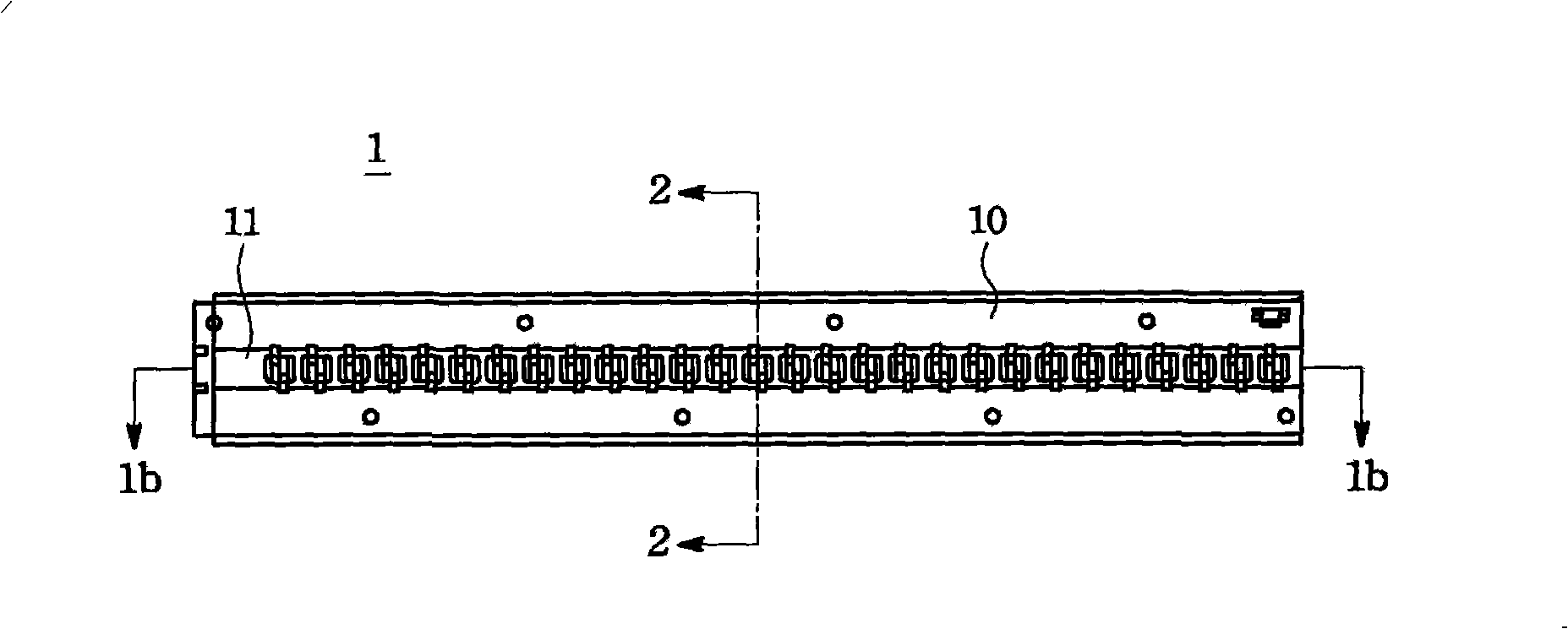
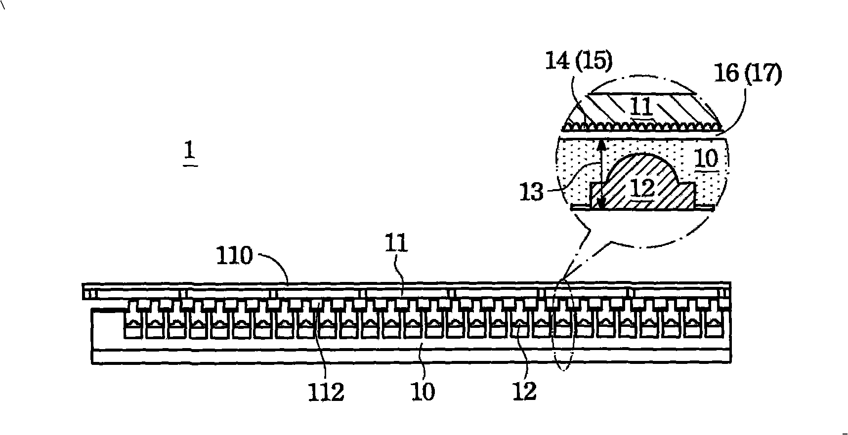
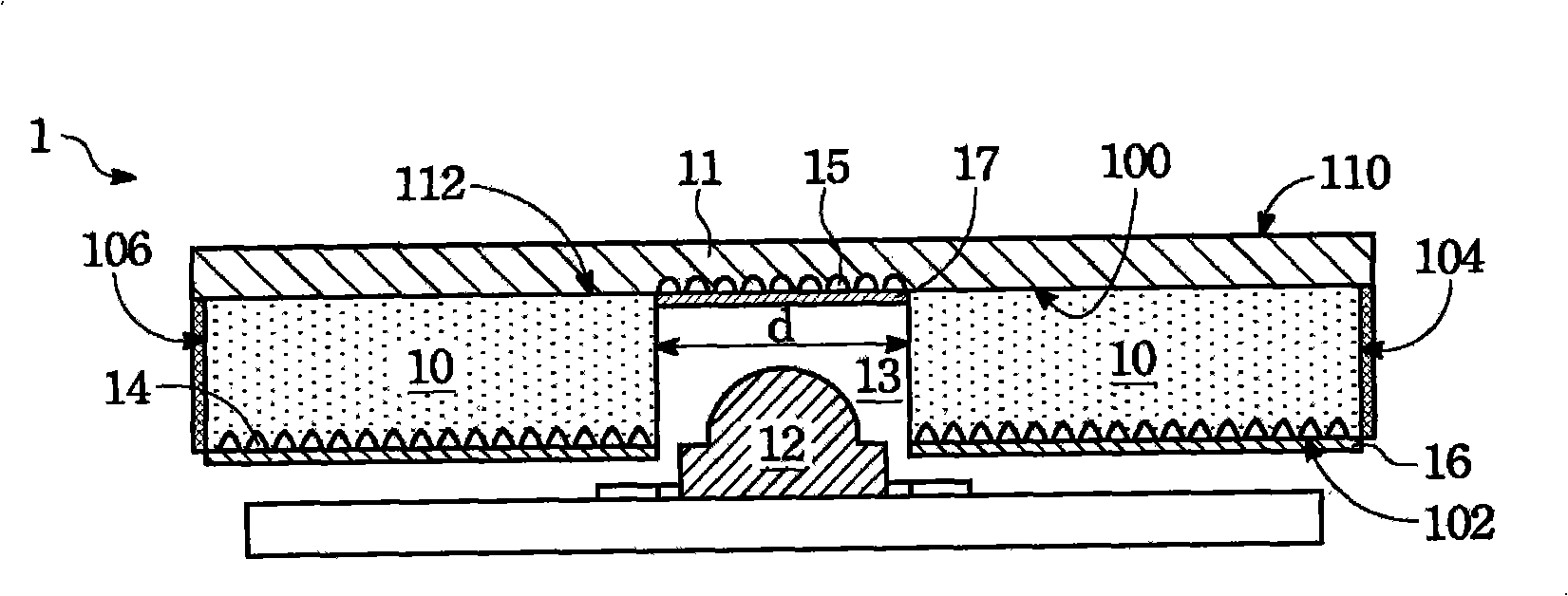
[0103] Figure 1A , Figure 1B Respectively represent the overall top view of the lighting device (Lighting device) according to the first embodiment of the present invention and the schematic cross-sectional view of the section line 1b-1b, figure 2 It means that the light-emitting device of the first embodiment of the present invention is Figure 1A In, 2-2 section schematic diagram of section line. As shown in the figure, the light emitting device 1 includes a plurality of elongated first light guide structures 10, a second light guide structure 11 and a light source 12, and the second light guide structure 11 is spliced ​​adjacent to two first light guide structures 10. , to accommodate the light source 12 into the space 13 formed by two adjacent first light guide structures 10 and the second light guide structure 11, wherein the bottom surface of the first light guide structure 10 on the same side as the light source 12 and the second light guide structure On the second ...

no. 2 example

[0112] For the light source lighting device of the second embodiment of the present invention, please refer to Figure 7 , Figure 8 and Figure 9 A schematic cross-sectional view of the light-emitting device shown. Let me explain here that the components and structures of this embodiment are roughly the same as those of the first embodiment, and the names and numbers of the components are also used in the first embodiment. The repetitions between this embodiment and the previous embodiment will not be described in detail. This only discloses the characteristics of this embodiment different from the previous embodiments, so as to further illustrate other implementations of the present invention. Such as Figure 7 As shown, the light source lighting device 2 of the second embodiment of the present invention includes a plurality of elongated first light guide structures 20, a second light guide structure 21 and at least one light source 22, and the thickness of the second lig...

no. 3 example

[0119] Figure 10 It is a schematic overall plan view of a Matrix / Array light emitting device according to the third embodiment of the present invention. The light-emitting device of this embodiment is a light-emitting device that uses a combination of a light guide plate, a reflective layer, and a light-emitting diode (Light Emitting Diodes, LED) light source to be used as a backlight source for a color liquid crystal display. Among them, the main structure of this embodiment is the same as that of the previous embodiments, and the components and structures of each part of the light-emitting device are substantially the same as those of the first embodiment, and the names of the components are also used above. Only the third embodiment is disclosed here that is different from the previous embodiments. characteristics, to further illustrate other embodiments of the present invention. Such as Figure 10 As shown, the array light-emitting device 3 of this embodiment includes a...


PUM


Abstract

The invention provides a light source light emitting device, a direct-type backlight module with the light-emitting device, a light box module, a planar light radiator, an LCD picture screen, a digital electronic device and a manufacturing method of the light-emitting device and the related products. The light emitting device comprises a plurality of long strip-shaped first light guide structures, a second light guide structure and a light source, the second light guide structure is adjacently spliced with two first light guide structures for receiving and containing the light source in a space which is combined by the two adjacent first light guide structures and the second light guide structure, wherein, patterned reflection layers are formed on the surfaces of the first light guide structures and the second light guide structure which are positioned at the same side of the light source and close to the periphery and the bottom part of the light source, at least optical reflection structures are additionally covered on the patterned reflection layers which are positioned at the bottom surfaces of the first light guide structures and the second light guide structure, thereby allowing light rays emitted by the light source to pass through the patterned reflection layers and the optical reflection structures for diffusion and reflection, improving the light uniformity, promoting the color mixing and reducing the occurrence of a dark band.

Description

technical field [0001] The invention relates to a light source light emitting device, an array light emitting device, a direct backlight module with a light emitting device, a planar light radiator (Planar Light Radiator), a liquid crystal image display screen (LCD PictureScreen), and digital electronic equipment with a light emitting device. And the manufacture method of above-mentioned each device. In particular, it involves the combination of a light guide plate, a reflective layer and a light emitting diode (Light Emitting Diodes, LED) strip or point light source as a backlight light source lighting device, and a direct-type backlight module that improves the light source scattering uniformity and RGB color mixing effect. A digital electronic device for a type backlight module and a manufacturing method thereof. Background technique [0002] As we all know, if the liquid crystal display (Liquid Crystal Display, LCD) picture is to be clear, since the liquid crystal itsel...

Claims


Application Information

Patent Timeline
Patent Type & Authority Applications(China)
IPC IPC(8): G02F1/13357G02B6/00G02B1/04G02F1/1335
Inventor 钟丰建
Owner CHI LIN OPTOELECTRONICS CO LTD
Why Eureka
Try Eureka