Isolation structure of shallow plough groove and manufacturing method thereof

A technology of isolation structure and manufacturing method, which is applied in the direction of semiconductor/solid-state device manufacturing, electrical components, circuits, etc., to achieve the effect of improving density and uniformity, increasing density and uniformity, and increasing density and uniformity

Inactive Publication Date: 2008-12-24
SEMICON MFG INT (SHANGHAI) CORP
View PDF1 Cites 28 Cited by
  • Summary
  • Abstract
  • Description
  • Claims
  • Application Information

AI Technical Summary

Problems solved by technology

Further enhancing the filling ability of trenches to achieve void-free and damage-free filling is still a huge challenge for the HDP-CVD process

Method used


Image

  • Isolation structure of shallow plough groove and manufacturing method thereof
  • Isolation structure of shallow plough groove and manufacturing method thereof
  • Isolation structure of shallow plough groove and manufacturing method thereof

Examples


Embodiment Construction

[0046] In order to make the above objects, features and advantages of the present invention more comprehensible, specific implementations of the present invention will be described in detail below in conjunction with the accompanying drawings. In the following description, numerous specific details are set forth in order to provide a thorough understanding of the present invention. However, the present invention can be implemented in many ways other than those described here, and those skilled in the art can make similar extensions without departing from the connotation of the present invention. Accordingly, the invention is not limited to the specific implementations disclosed below.

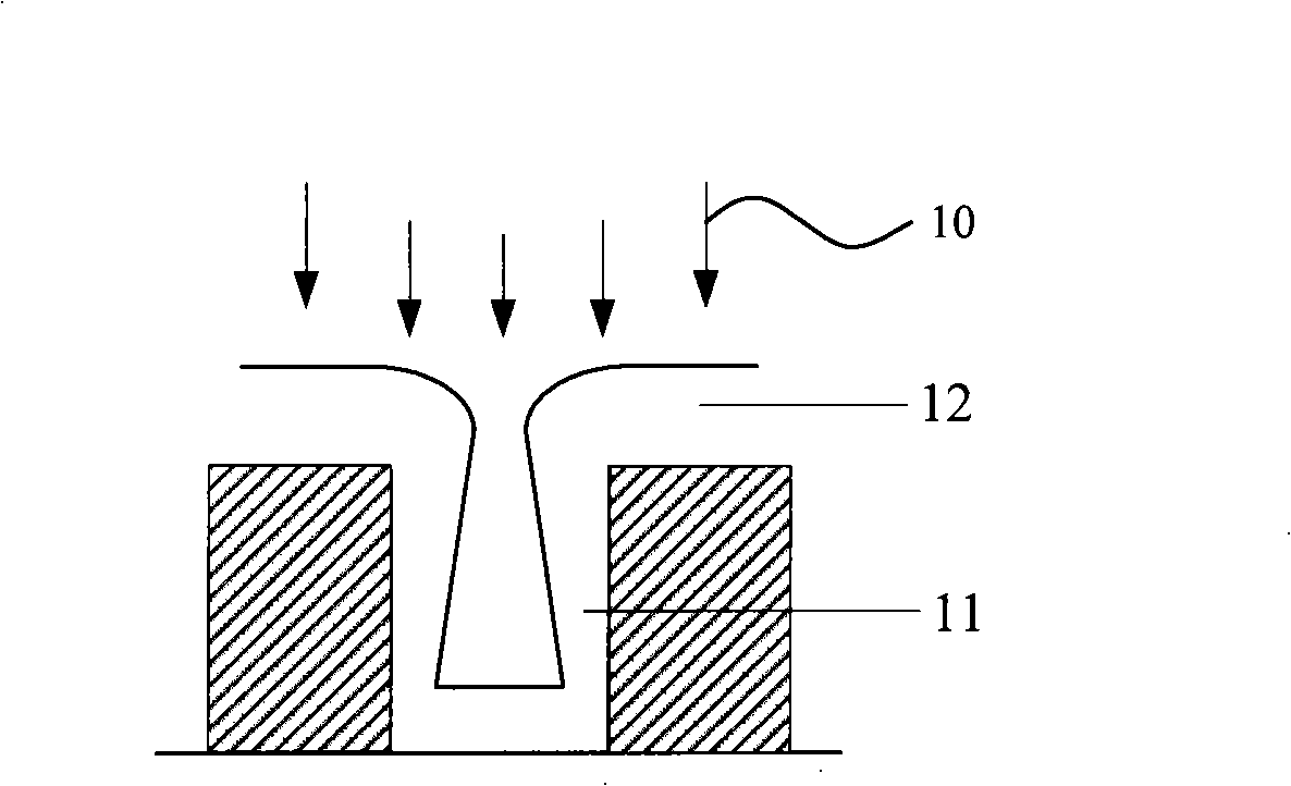
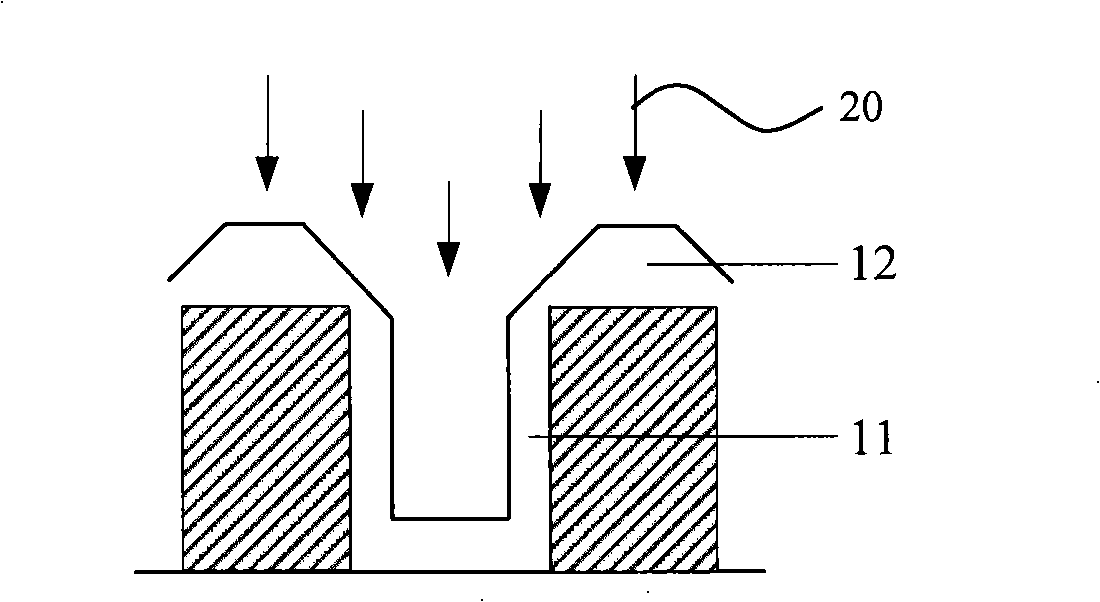
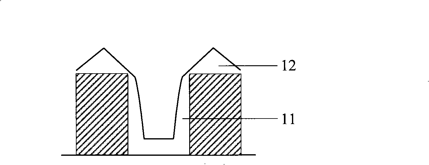
[0047] The invention relates to the technical field of semiconductor integrated circuit manufacturing, in particular to a method for forming a shallow trench isolation structure in a semiconductor device and the shallow trench isolation structure. It should be noted here that this specificatio...


PUM


Abstract

The invention discloses a manufacturing method of a shallow groove isolating structure, which comprises the following steps of: providing a semiconductor underlay; forming a mat oxide layer and a mat azotization layer on the surface of the semiconductor underlay; carrying out the etch of the mat oxide layer, the mat azotization layer and the semiconductor underlay so as to form grooves; carrying out the sedimentation of a first medium layer at the grooves and the surface of the underlay by a first high density plasma chemical gas deposition technology; and carrying out high-temperature thermal annealing and introduction of oxygen to form a silicon oxide layer on the surface of the first medium layer; carrying out the sedimentation of a second medium layer on the surface of the silicon oxide layer by a second high density plasma chemical gas deposition technology; carrying out rapid thermal annealing; grinding the first medium layer and the second medium layer to the mat azotization layer; and removing the mat azotization layer and the mat oxide layer. The STI isolating structure and the manufacturing method of the invention can realize void-free and zero-defect filling of a high depth-width ratio STI isolating groove.

Description

technical field [0001] The invention relates to the technical field of semiconductor manufacturing, in particular to a shallow trench isolation (STI) structure and a manufacturing method thereof. Background technique [0002] With the rapid development of semiconductor technology, the feature size of semiconductor devices has been significantly reduced, and correspondingly higher requirements have been put forward for the chip manufacturing process. One of the challenging issues is to fill the insulating dielectric uniformly and non-porously between the various film layers or in the trenches to provide sufficient and effective isolation protection. After the manufacturing process enters the deep submicron technology node, shallow trench isolation (shallow trench isolation, STI) structure has been mostly adopted for the isolation between the active regions of components below 0.13 μm, such as MOS devices. The formation of the STI isolation structure first needs to etch a tre...

Claims


Application Information

Patent Timeline
Patent Type & Authority Applications(China)
IPC IPC(8): H01L21/762
CPCH01L21/76224
Inventor 刘永肖德元
Owner SEMICON MFG INT (SHANGHAI) CORP
Why Eureka
Try Eureka