Method of manufacturing mask for semiconductor device
A semiconductor and mask technology, used in semiconductor/solid-state device manufacturing, originals for opto-mechanical processing, and photolithography processes for patterned surfaces, which can solve the degradation of wafer yield, the impact of production time, and the increase in time consumption and cost. And other issues
- Summary
- Abstract
- Description
- Claims
- Application Information
AI Technical Summary
Problems solved by technology
Method used
Image

Examples
Embodiment Construction
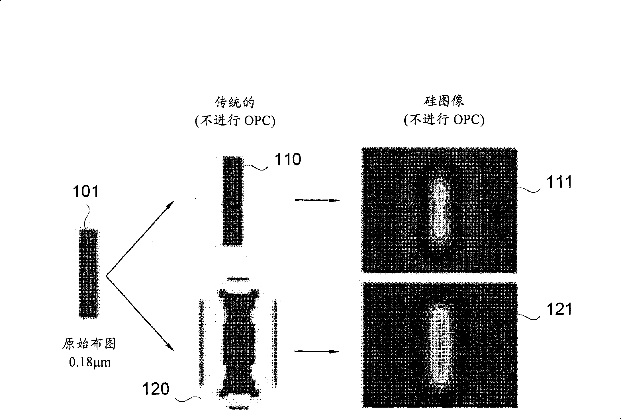
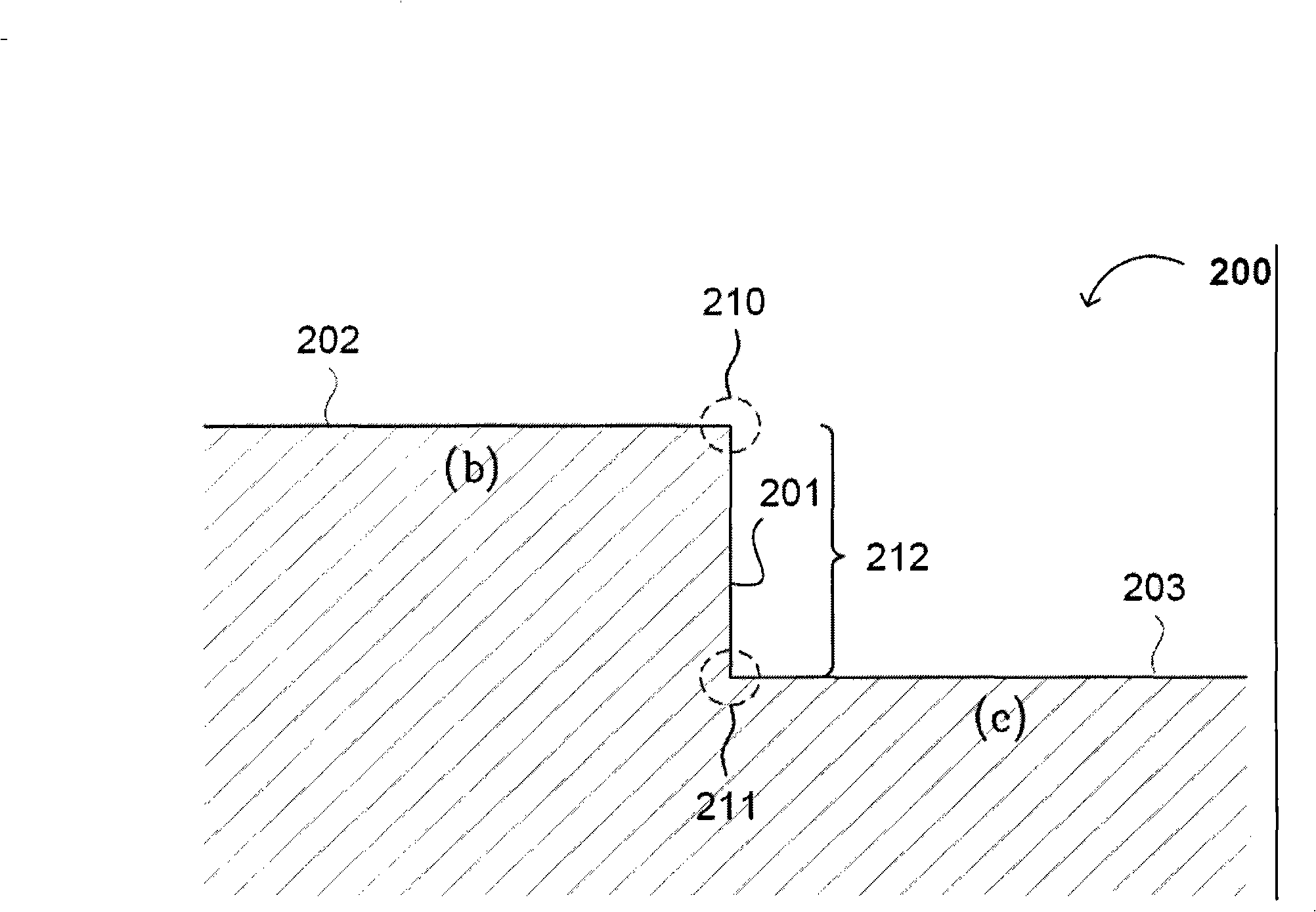
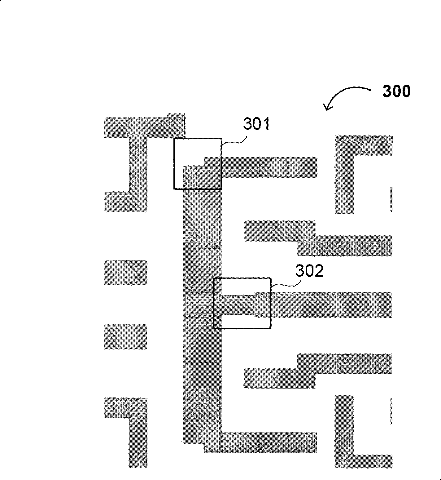
[0038] Preferred embodiments and examples of the present invention will be described in detail with reference to the accompanying drawings. Wherever possible, the same reference numbers will be used throughout the drawings to refer to the same or like parts.
[0039] Figure 4 is a flowchart illustrating an exemplary method of fabricating a mask using optical proximity correction a1 (OPC). First, a design database input step (S402) is implemented to input the design database into the mask manufacturing process. For example, after tape-out, the design database can be transferred to a semiconductor manufacturing facility (FAB) to implement the process based on the FAB's manufacturing capabilities.
[0040] Implement the design rule detection (DRC) step (S404), whether the input data of detection layout exceeds (drawn) the design rule that follows, if find the design error against this design rule or implement the layout correction step (S406) that violates the rule and correct...
PUM
 Abstract
Description
Claims
Application Information