High doping point electrode SOI piezoresistance type pressure sensor and manufacturing method thereof

A technology of a pressure sensor and a manufacturing method, which is applied in the direction of fluid pressure measurement by changing ohmic resistance, measurement of the property force of piezoelectric resistance materials, instruments, etc., can solve the problems of long metal electrodes and reduced reliability, and achieve Effects of reduced leakage current, improved reliability, and high precision

Inactive Publication Date: 2009-01-21
NO 49 INST CHINESE ELECTRONICS SCI & TECH GRP
View PDF0 Cites 23 Cited by
  • Summary
  • Abstract
  • Description
  • Claims
  • Application Information

AI Technical Summary

Problems solved by technology

[0003] In order to solve the problem that the length of the metal electrode used is long and the reliability of the product is reduced for h...

Method used


Image

  • High doping point electrode SOI piezoresistance type pressure sensor and manufacturing method thereof
  • High doping point electrode SOI piezoresistance type pressure sensor and manufacturing method thereof
  • High doping point electrode SOI piezoresistance type pressure sensor and manufacturing method thereof

Examples


specific Embodiment approach 1

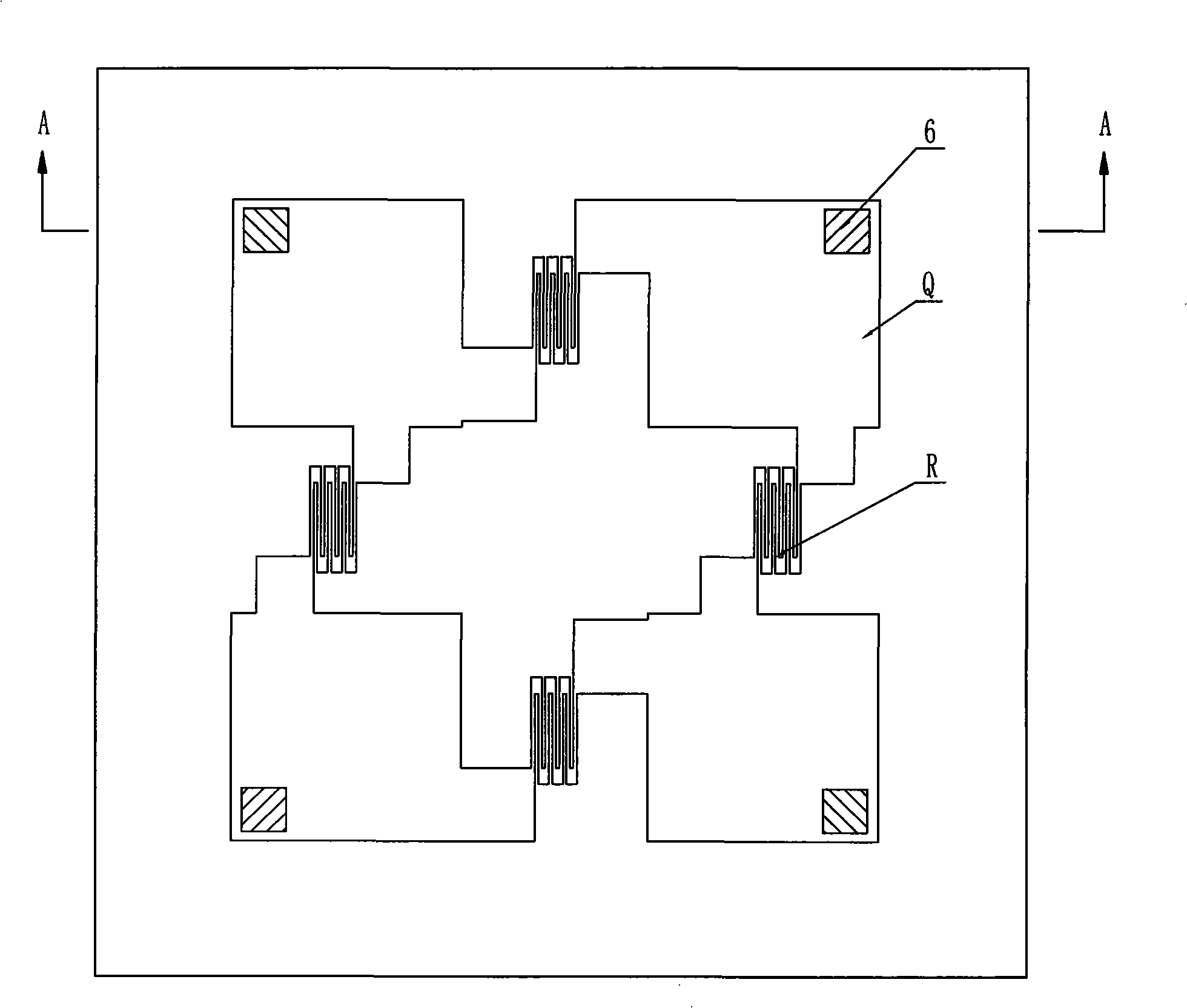
[0019] Specific implementation mode one: combine figure 1 and Fig. 9 illustrate the present embodiment, the highly doped point electrode SOI piezoresistive pressure sensor of the present embodiment consists of a silicon substrate 1, a first silicon dioxide layer 2, a thin silicon dioxide layer 3, a second silicon dioxide layer 4. A silicon nitride layer 5, an electrode 6 and a highly doped layer 7; the silicon substrate 1, the first silicon dioxide layer 2 and the highly doped layer 7 constitute an SOI diaphragm sequentially from bottom to top; A thin silicon dioxide layer 3, a second silicon dioxide layer 4 and a silicon nitride layer 5 are sequentially oxidized and grown on the outside of the SOI diaphragm from the inside to the outside; the highly doped layer 7 and the upper thin silicon dioxide layer 3 Etched into the pattern of the highly doped region Q and the sensitive resistor R, the electrode 6 penetrates the upper second silicon dioxide layer 4, the upper silicon nit...

specific Embodiment approach 2

[0020] Specific implementation mode two: combination figure 2 Referring to FIG. 9 to illustrate this embodiment, the manufacturing steps of the highly doped point electrode SOI piezoresistive pressure sensor are as follows:

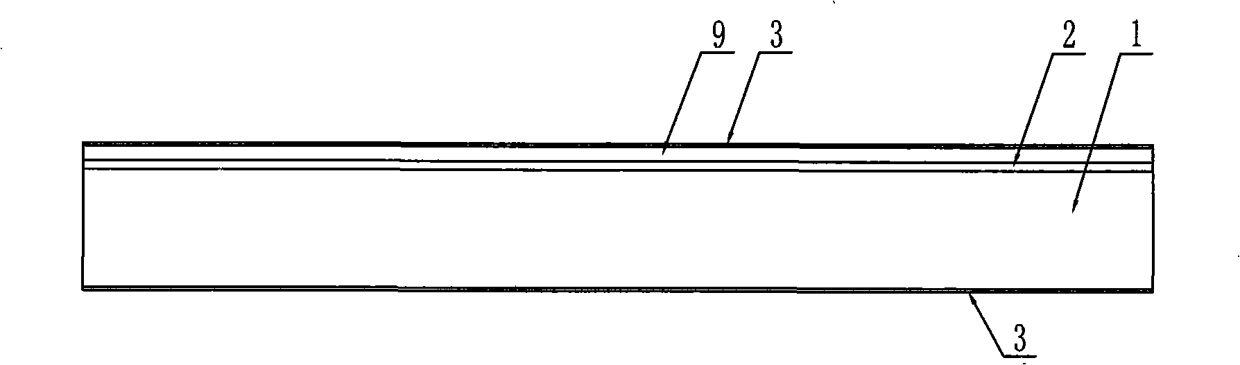
[0021] Step 1: Clean and oxidize the SOI diaphragm composed of the silicon substrate 1, the first silicon dioxide layer 2 and the device layer 9 to form a thin silicon dioxide layer 3 with a thickness of 50 nm; the first silicon dioxide layer 2 As a buffer layer injected with concentrated boron; cleaning is carried out by standard cleaning process of semiconductor planar technology;

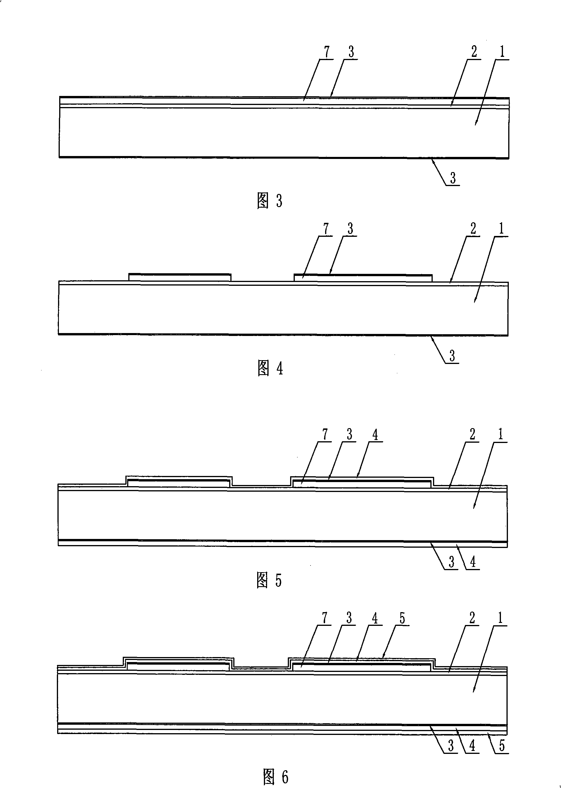
[0022] Step 2: As shown in FIG. 3 ; implant the device layer 9 with a concentration of 2×10 through a large beam implanter 20 cm -3 , implanting concentrated boron with an energy of 80 keV to form a highly doped layer 7;

[0023] Step 3: As shown in Figure 4; photolithography and etching are carried out on the highly doped layer 7 and the thin silicon dioxide layer 3 to ...


PUM

PropertyMeasurementUnit
Thicknessaaaaaaaaaa
Thicknessaaaaaaaaaa
Thicknessaaaaaaaaaa

Abstract

The invention relates to a highly-doped pointed electrode SOI piezoresistive pressure sensor and a manufacturing method thereof, namely a piezoresistive pressure sensor. The piezoresistive pressure sensor solves the problems that the length of a metal electrode is longer and the reliability of products is lowered through utilizing in high temperature. A SOI diaphragm is formed by a silicon substrate, a first silicon dioxide layer and a highly-doped layer. A thin silicon layer, a second silicon layer and a silicon nitride layer are arranged on the outer portion of the piezoresistive pressure sensor from inside to outside in turn. An electrode is bonded with the highly-doped layer through the upper three layers, and the silicon substrate and the lower three layers are corroded to form a bottom groove. The manufacturing method comprises the flowing steps in turn: injecting heavy boron in the SOI diaphragm, etching to form a highly-doped area Q and a sensitive resistance R, secondarily oxygenizing, generating silicon nitride, and then, making a lead wire and etching the bottom groove, and finally, finishing the conventional process. The sensitive resistor and the lead wire are made through adopting a highly-doped technique, independent high doping is not needed to be done on the extraction portion of an electrode to do ohmic contact, and meanwhile, an annealing process is reduced, the production cost is lowered, and the reliability of products is improved.

Description

technical field [0001] The invention relates to a piezoresistive pressure sensor. Background technique [0002] Existing piezoresistive pressure sensors are mainly made of single crystal silicon materials, and the pressure sensitive resistor is isolated from the substrate by a PN junction. Due to the inherent properties of the PN junction itself, its operating temperature range is narrow , which limits the range of use of this type of sensor. In addition, due to the existence of the PN junction, there is inevitably a certain leakage current, which makes the stability of the sensor worse. For the SOI piezoresistive pressure sensor that cancels the PN junction, if it is manufactured with a low-doping process, it needs to be highly doped for ohmic contact at the lead-out of the electrode. At the same time, the annealing process and process steps are increased, which increases the cost and reduces In order to reduce the reliability of the product, this kind of sensor can only u...

Claims


Application Information

Patent Timeline
IPC IPC(8): G01L1/18G01L1/22G01L9/06
Inventor 田雷金建东齐虹于海超尹延昭李海博王永刚付博寇文兵王江
Owner NO 49 INST CHINESE ELECTRONICS SCI & TECH GRP
Why Eureka
Try Eureka