Semiconductor test management system

A test management and semiconductor technology, applied in the direction of single semiconductor device testing, electronic circuit testing, measuring electricity, etc., can solve the problems of error-prone test efficiency, many steps, complicated procedures, etc., so as to improve the detection accuracy and simplify the detection procedure. , the effect of improving the detection efficiency

Inactive Publication Date: 2009-01-21
SEMICON MFG INT (SHANGHAI) CORP
View PDF0 Cites 11 Cited by
  • Summary
  • Abstract
  • Description
  • Claims
  • Application Information

AI Technical Summary

Problems solved by technology

[0004] However, from the above-mentioned wafer testing process, we can find that the above-mentioned testing process has many steps, the procedure is complicated, and there are many manual operations, which are prone to errors and low testing efficiency.

Method used


Image

  • Semiconductor test management system
  • Semiconductor test management system
  • Semiconductor test management system

Examples


Embodiment Construction

[0022] The semiconductor test management system of the present invention will be further described in detail below in conjunction with the accompanying drawings.

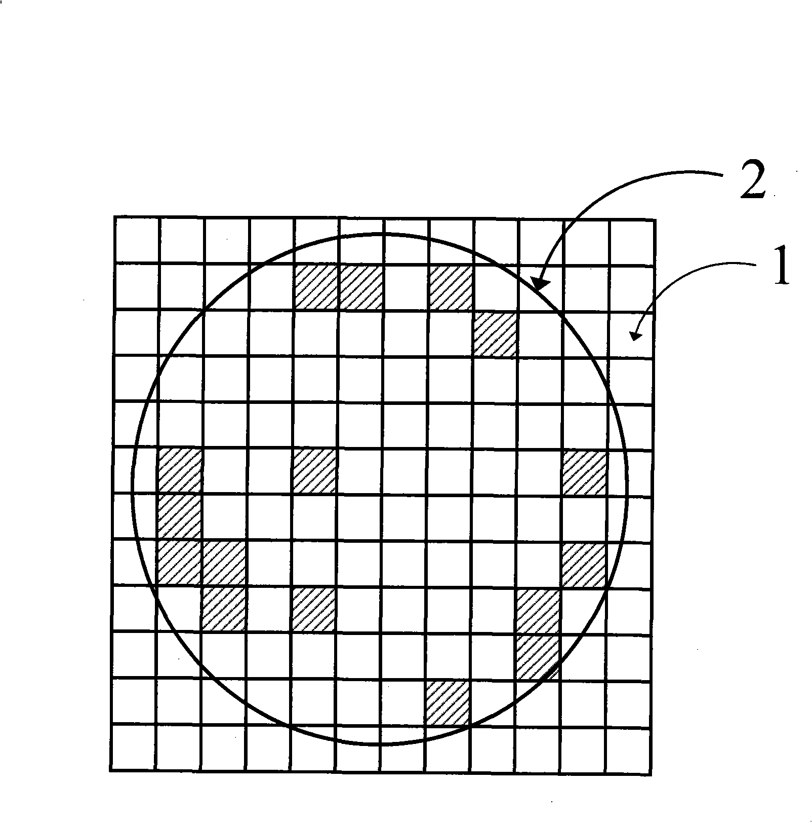
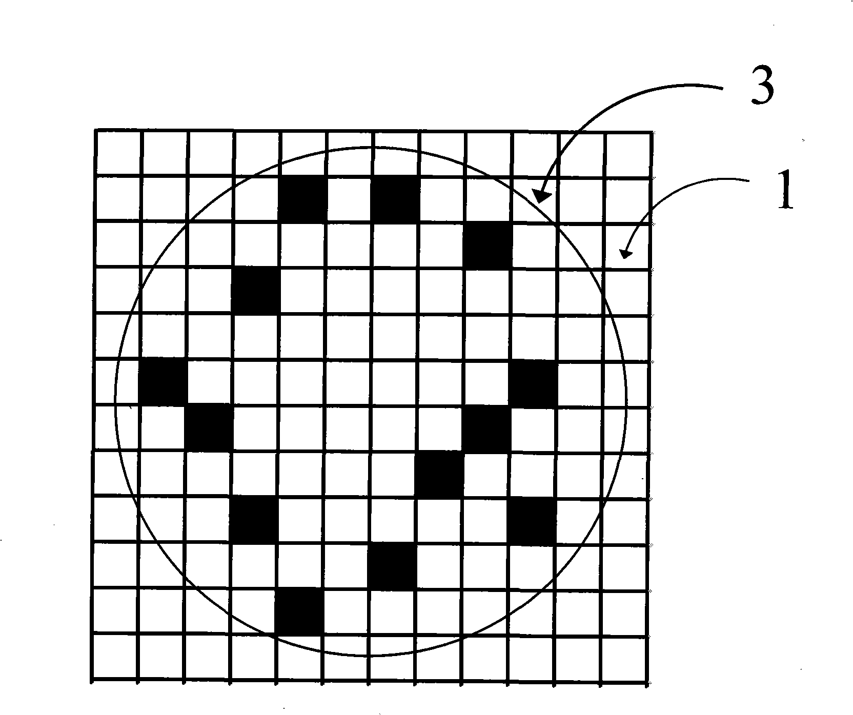
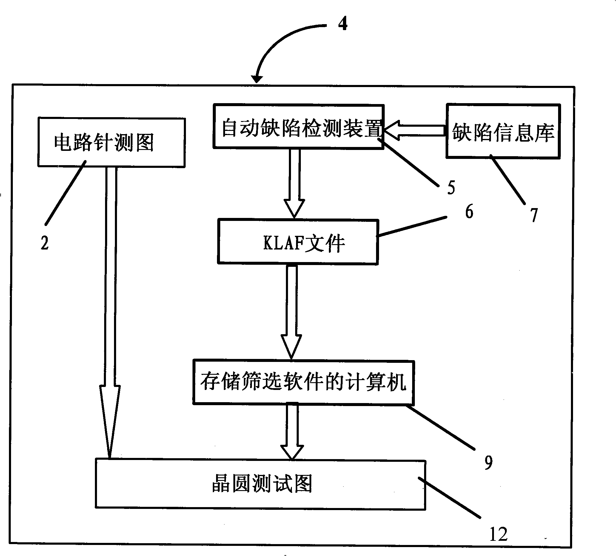
[0023] like Figure 4 As shown, the semiconductor test management system 4 of the present invention includes: a circuit needle test figure 2 , the circuit pin test figure 2 It is a diagram of the results of the wafer probe card using the probe to detect the electrical characteristics of each die on the wafer. Among them, the unqualified die will be tested on the circuit needle. figure 2 Superscript on the mark, such as figure 1 As shown, the shaded area is a disqualified grain, and the unqualified grain marked with the mark will be eliminated, so as not to increase the manufacturing cost; an automatic defect detection device 5 (Auto Inspection Tool, AVI tool), wherein the automatic detection device 5 is The defect detection device produced by Cametak can scan and detect all the defects of the wafer at one time a...


PUM


Abstract

The invention relates to a semiconductor test management system, comprising a circuit probe detection map recording the electricity property of a wafer; an automatic defect detection device detecting the defects of the wafer and a computer storing selection software, wherein the selection software contains selection standards for selecting the defects of the wafer. The semiconductor test management can detect the defects of wafers, simplifies test program and adopts computer to improve test efficiency.

Description

technical field [0001] The invention relates to a semiconductor test management system, in particular to a semiconductor test management system used for wafer circuit needle testing and defect detection. Background technique [0002] In the semiconductor manufacturing process, semiconductor wafers usually go through a series of processes, such as exposure, chemical mechanical polishing, chemical vapor deposition, etching, wafer testing, dicing, packaging, and the like. For example, a 15-micron semiconductor product may go through nearly 600 processing steps, among which wafer testing is an important and indispensable part of the semiconductor industry chain, which runs from the beginning of product design to the completion of processing the whole process. [0003] General wafer testing includes circuit probe (CP) and defect detection. The circuit needle test is to detect the electrical characteristics of each die on the wafer 1, so as to detect and eliminate unqualified di...

Claims


Application Information

Patent Timeline
Patent Type & Authority Applications(China)
IPC IPC(8): G01R31/00G01R31/01G01R31/26G01R31/28
Inventor 吕秋玲许俊庄祈龙王明珠
Owner SEMICON MFG INT (SHANGHAI) CORP
Why Eureka
Try Eureka