

Optical device, method for producing master for use in producing optical device, and photoelectric conversion apparatus
A technology for optical elements and manufacturing methods, which is applied in the direction of optical elements, optical elements, and exposure devices for photolithography, and can solve the problems of impractical anti-reflection structures, inability to achieve low reflectivity, and poor wavelength-dependent characteristics of reflectivity. Excellent light utilization efficiency, improved anti-reflection characteristics, and less surface reflection
- Summary
- Abstract
- Description
- Claims
- Application Information
AI Technical Summary
Problems solved by technology
Method used
Image

Examples
no. 1 example
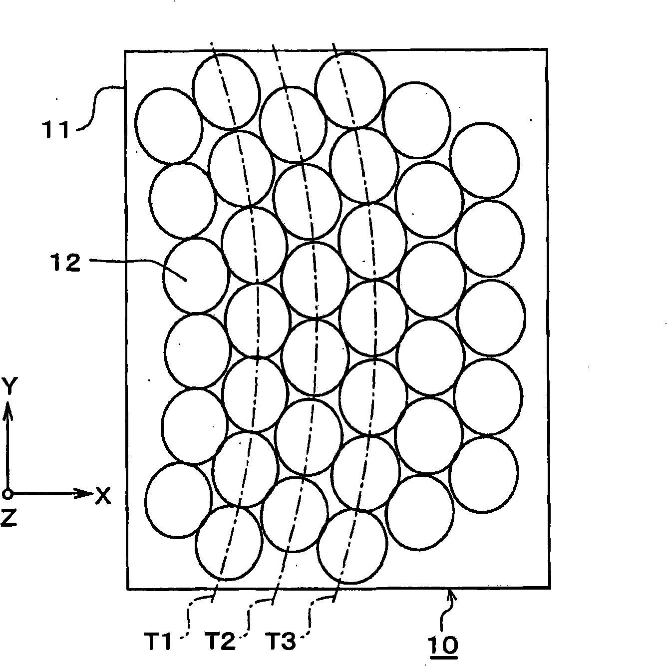
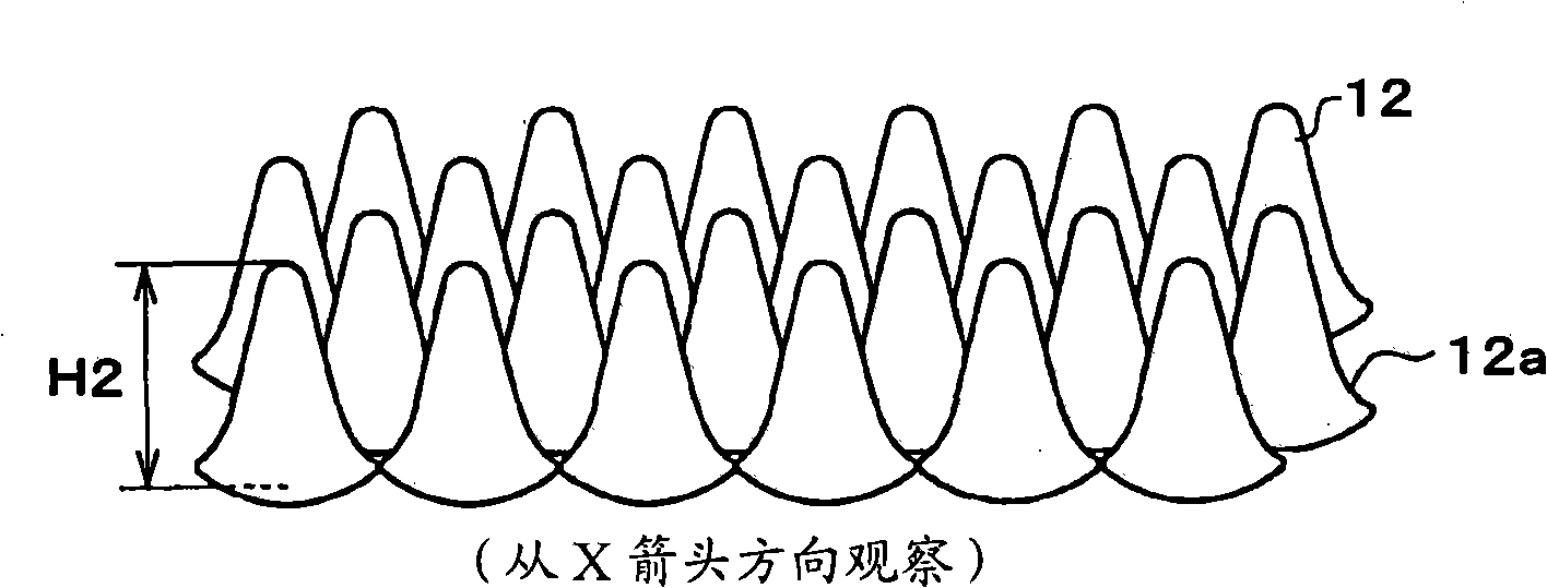
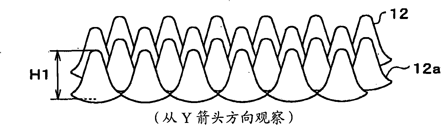
[0075] FIG. 1 is a schematic configuration diagram of an optical element 10 according to a first embodiment of the present invention. here, Figure 1A is a plan view of the main part of the optical element 10; Figure 1B From Figure 1A The perspective view of the main part of the X direction observation optical element 10; Figure 1C From Figure 1A The perspective view of the main part of the optical element 10 observed in the Y direction of .
[0076]The optical element 10 of this embodiment has a structure (sub-wavelength structure) in which a plurality of structures formed of protrusions are arranged on the surface of the substrate 11 at fine pitches equal to or less than the wavelength of visible light. Body 12. Here, the wavelength of visible light or less means a wavelength of about 400 nm or less. The optical element 10 has the following functions: prevent edge Figure 1A The light transmitted through the substrate 11 in the Z direction is reflected at the inte...
no. 2 example
[0127] Next, a second embodiment of the present invention will be described.
[0128] FIG. 7 is a cross-sectional view for explaining schematic steps of main parts of a method of manufacturing an optical element having a subwavelength structure having the above-described structure formed on both surfaces of a substrate 11 . FIG. 7A shows the process of forming a pattern of a resist layer 2 on the surface of a quartz substrate 1, and FIG. 7B shows an etching process using the patterned resist layer 2 as a mask to make a pattern on the substrate 1. The process of producing a master disk 4 for optical element production with a concavo-convex structure including recesses 3 on its surface. FIG. FIG. 7D shows the manufacturing process of the metal mold 9 for optical element production obtained by peeling off the replica substrate 8 after electroplating a conductive film on the uneven structure surface of the replica substrate 8 .
[0129] In this embodiment, two metal molds 9 manufac...
no. 3 example
[0133] Figure 8 A third embodiment of the invention is shown. In this embodiment, a dye-sensitized solar cell 50 using the optical element 40 whose structure has been described in the above-mentioned second embodiment as a conductor will be described as an example. light window.
[0134] The dye-sensitized solar cell 50 of this embodiment is composed of a laminated body in which a metal oxide semiconductor 45 and an electrolyte layer 46 are provided between a conductive window 40 and a substrate 44, wherein the conductive window 40 includes a transparent conductive film 41, and the substrate 44 includes a (transparent) conductive film 42 that is opposite to the transparent conductive film 41 , and a current collecting member 43 . The semiconductor layer 45 includes, for example, an oxide semiconductor material and a sensitizing dye. In addition, the transparent conductive film 41 and the conductive film 42 are connected by wires, and a current circuit having an ammeter 47 ...
PUM
| Property | Measurement | Unit |
|---|---|---|
| wavelength | aaaaa | aaaaa |
| depth | aaaaa | aaaaa |
| depth | aaaaa | aaaaa |
Abstract
Description
Claims
Application Information