Circuit board construction embedded with semi-conductor chip and preparation thereof

A conductive structure and semiconductor technology, applied in semiconductor/solid-state device manufacturing, semiconductor devices, semiconductor/solid-state device components, etc., can solve problems such as electrical quality problems, surface oxidation of connecting metal layers, etc.

Active Publication Date: 2012-05-16
UNIMICRON TECH CORP
View PDF0 Cites 0 Cited by
  • Summary
  • Abstract
  • Description
  • Claims
  • Application Information

AI Technical Summary

Problems solved by technology

[0004] Although the above-mentioned prior art can form a connection metal layer on the surface of the electrode pad to avoid oxidation of the electrode pad, and can avoid contamination of the electrode pad on the surface of the semiconductor chip during the subsequent semiconductor chip packaging process, the connection metal layer is usually Formed by electroplating of copper (Cu) material, if exposed to the air, it will cause the surface oxidation of the connecting metal layer and cause electrical quality problems

Method used


Image

  • Circuit board construction embedded with semi-conductor chip and preparation thereof
  • Circuit board construction embedded with semi-conductor chip and preparation thereof
  • Circuit board construction embedded with semi-conductor chip and preparation thereof

Examples


Embodiment Construction

[0034] The implementation of the present invention is described below through specific specific examples, and those skilled in the art can easily understand other advantages and effects of the present invention from the content disclosed in this specification.

[0035] Figure 2A to Figure 2G A schematic cross-sectional view of a preferred embodiment of the method of manufacturing a semiconductor chip-embedded circuit board structure of the present invention will be described in detail.

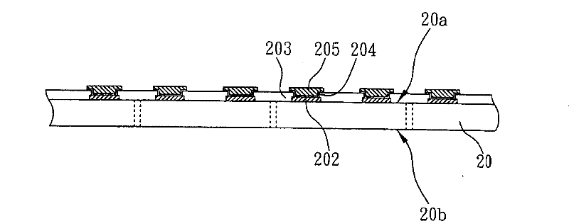
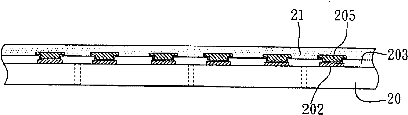
[0036] Such as Figure 2A As shown, at first, a semiconductor chip 20 having an active surface 20a and a non-active surface 20b opposite to the active surface 20a is provided, and the active surface 20a has a plurality of electrode pads 202 on the surface of the active surface 20a of the semiconductor chip 20 A passivation protection layer 203 (Passivation layer) is formed, an opening 204 is formed on the surface of the passivation protection layer 203 to expose the electrode pad 202 of the ...


PUM


Abstract

A circuit board buried in a semiconductor chip and a fabrication method thereof are disclosed, mainly aiming at providing a semiconductor wafer which has an active face. The active face is provided with a plurality of electrode pads on which a connecting metal layer is formed; a protective layer is developed on the surface of the connecting metal layer and on the surface of the semiconductor wafer; and a plurality of semiconductor chips are formed through cutting process. A carrier plate provided with at least one opening is provided so as to connect and arrange the semiconductor chips in theopening; a dialectic layer and a circuitry layer are sequentially developed on the protective layer on the surfaces of the semiconductor chips and on the carrier plate; and the circuitry layer is electrically connected to the connecting metal layer of the semiconductor chips. Therefore, the invention can protect the connecting metal layer covered by the protective layer arranged on the surfaces of the semiconductor chips from oxidation and contamination and has the advantage that the invention can simplify technique and reduce cost and short processing time.

Description

technical field [0001] The invention relates to a structure of a circuit board embedded with a semiconductor chip and a manufacturing method thereof, in particular to a structure of embedding a semiconductor chip into a circuit board and a manufacturing method thereof. Background technique [0002] In order to meet the market demand, the semiconductor packaging structure strives to be light, thin and short, and the chip is also developing towards small size and high integration (Integration). In view of this, the circuit board as the chip carrier (Chip carrier) is preferably equipped with high-density electrical connection pads. So that the semiconductor chip carried on the circuit board can form a good and complete electrical connection with the circuit board, so that the highly integrated semiconductor chip can operate freely and fully exert its functions and characteristics. Therefore, the ball grid array (BGA) structure, flip chip (Flip Chip) structure, chip size package...

Claims


Application Information

Patent Timeline
Patent Type & Authority Patents(China)
IPC IPC(8): H01L23/488H01L23/498H01L23/492H01L23/13H01L21/60H05K1/18H05K3/32
CPCH01L24/19H01L2224/04105H01L2224/19H01L2924/14H01L2924/18162H01L2924/00H01L2924/00012
Inventor 胡竹青陈尚玮
Owner UNIMICRON TECH CORP
Why Eureka
Try Eureka