Capacitor embedded semi-conductor package substrate construction and preparation thereof

A technology for packaging substrates and capacitor components, which is used in the manufacture of semiconductor/solid-state devices, assembling printed circuits with electrical components, and electrical components. Precise, material-saving effects

Inactive Publication Date: 2009-02-11
PHOENIX PRECISION TECH CORP
View PDF0 Cites 12 Cited by
  • Summary
  • Abstract
  • Description
  • Claims
  • Application Information

AI Technical Summary

Problems solved by technology

[0004] However, the cost of laminating the whole piece of high dielectric material in this method is quite high, and if only a small area is used, it will cause material waste
In addition, there will be a problem of hole filling, because the whole piece of high dielectric material has poor glue f

Method used


Image

  • Capacitor embedded semi-conductor package substrate construction and preparation thereof
  • Capacitor embedded semi-conductor package substrate construction and preparation thereof
  • Capacitor embedded semi-conductor package substrate construction and preparation thereof

Examples


Embodiment 1

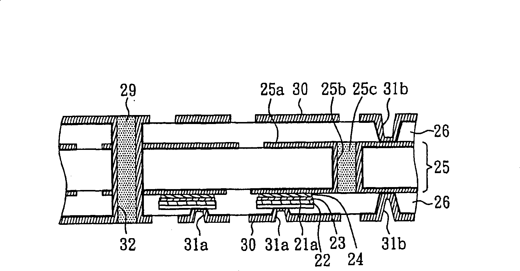
[0047] Please refer to figure 2 , is a cross-sectional view of the capacitive element embedded in the semiconductor package substrate structure of the present invention. like figure 2 As shown, an inner circuit board 25 , a dielectric layer 26 , and an outer circuit layer 30 are included. There is an inner layer circuit layer 25a in the inner layer circuit board 25, and the inner layer circuit layer 25a is a copper layer, and the inner layer circuit board 25 may also include an inner plating via hole 25b, the inner plating via hole 25b further includes an insulating resin 25c, and the material of the inner wall is copper, so as to be connected to the inner circuit layer 25a on both sides of the inner circuit board 25 . The dielectric layer 26 is disposed on both sides of the inner circuit board 25, and the materials used may be ABF (Ajinomoto Build-up Film), BCB (Benzocyclo-buthene), LCP (Liquid Crystal Polymer), PI (Poly-imide ), PPE (Poly (phenylene ether)), PTFE (Poly ...

Embodiment 2

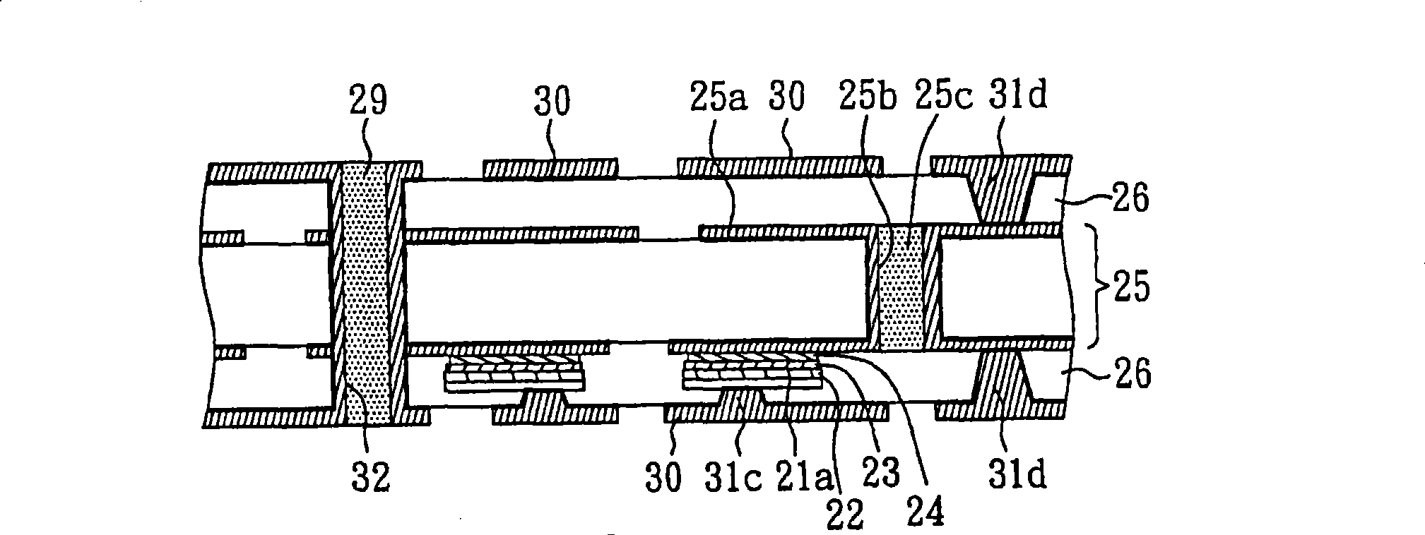
[0050] Please refer to image 3 , is a cross-sectional view of the capacitive element embedded in the semiconductor package substrate structure of the present invention. like image 3 As shown, its structure is substantially the same as that of Embodiment 2, but the difference is that the first conductive blind hole 31c and the second conductive blind hole 31d of this embodiment are filled with material, that is, filled with copper metal.

Embodiment 3

[0052] The materials used in this embodiment can be the same as those in Embodiment 1. This embodiment mainly lies in the production method, please refer to Figures 4A to 4H ', is a cross-sectional view of a method of manufacturing a semiconductor package substrate with an embedded selective capacitive element.

[0053] like Figure 4A As shown, firstly, a metal carrier 21 is provided, the material used in the metal carrier 21 can be a copper plate, and a plurality of capacitive materials 22 are selectively formed on its surface by coating or printing, and then these capacitive materials 22 An electrode layer 23 is formed on the surface in the same way, and a capacitor element can be formed after high-temperature sintering.

[0054] Next, if Figure 4B As shown, a fusible metal adhesive layer 24 is formed on the electrode layer 23 by screen printing. Another example Figure 4C As shown, the capacitive element is soldered back to the inner circuit layer 25 a of the inner ...


PUM


Abstract

The invention relates to a semiconductor encapsulated baseplate structure, in which a capacitance component is embedded. The structure comprises an inner layer circuit board, a dielectric layer and an outer circuit layer, wherein, the dielectric layer is disposed on both sides of the inner layer circuit board and provided with a first conductive blind hole which is communicated with the inner layer circuit board through a thin metal layer, a capacitance material, an electrode layer and an adhesive layer in sequence; the external circuit layer is disposed on the surface of the dielectric layer; and herein, the thin metal layer, the capacitance material and the electrode layer are taken as a capacitance component. The invention further provides a method for manufacturing the semiconductor encapsulated baseplate structure. Compared with the capacitance material formed by compressing the whole piece of high-dielectric material, the capacitance component embedded in the semiconductor encapsulated baseplate has the advantages of saving material, solving the pore-filling problem and avoiding creepage of the capacitance between circuits.

Description

technical field [0001] The invention relates to a capacitive element embedded semiconductor packaging substrate structure and its manufacturing method, especially to a capacitive element embedded semiconductor packaging substrate structure and its manufacturing method which are suitable for improving the leakage phenomenon of capacitor materials and the phenomenon of pores and uneven thicknesses. . Background technique [0002] Due to the progress of semiconductor manufacturing process and the continuous improvement of circuit functions on semiconductor chips, the development of semiconductor devices is becoming highly integrated. However, with the integration of semiconductor devices, the number of pins in the packaging structure also increases, and the noise also increases due to the increase in the number of pins and wiring. Therefore, in order to eliminate noise or make electrical compensation, passive elements, such as resistive elements, capacitive materials, and indu...

Claims


Application Information

Patent Timeline
IPC IPC(8): H01L23/488H01L23/492H01L23/498H01L25/00H01L21/60H01L21/48H05K1/16H05K3/30H05K3/42
CPCH01L2924/15311H01L2224/16225
Inventor 连仲城杨智贵
Owner PHOENIX PRECISION TECH CORP
Why Eureka
Try Eureka