

Semiconductor device and method of manufacturing the same
A semiconductor and device technology, applied in the field of semiconductor devices, can solve problems such as inability to achieve driving performance
- Summary
- Abstract
- Description
- Claims
- Application Information
AI Technical Summary
Problems solved by technology
Method used
Image

Examples
no. 1 example
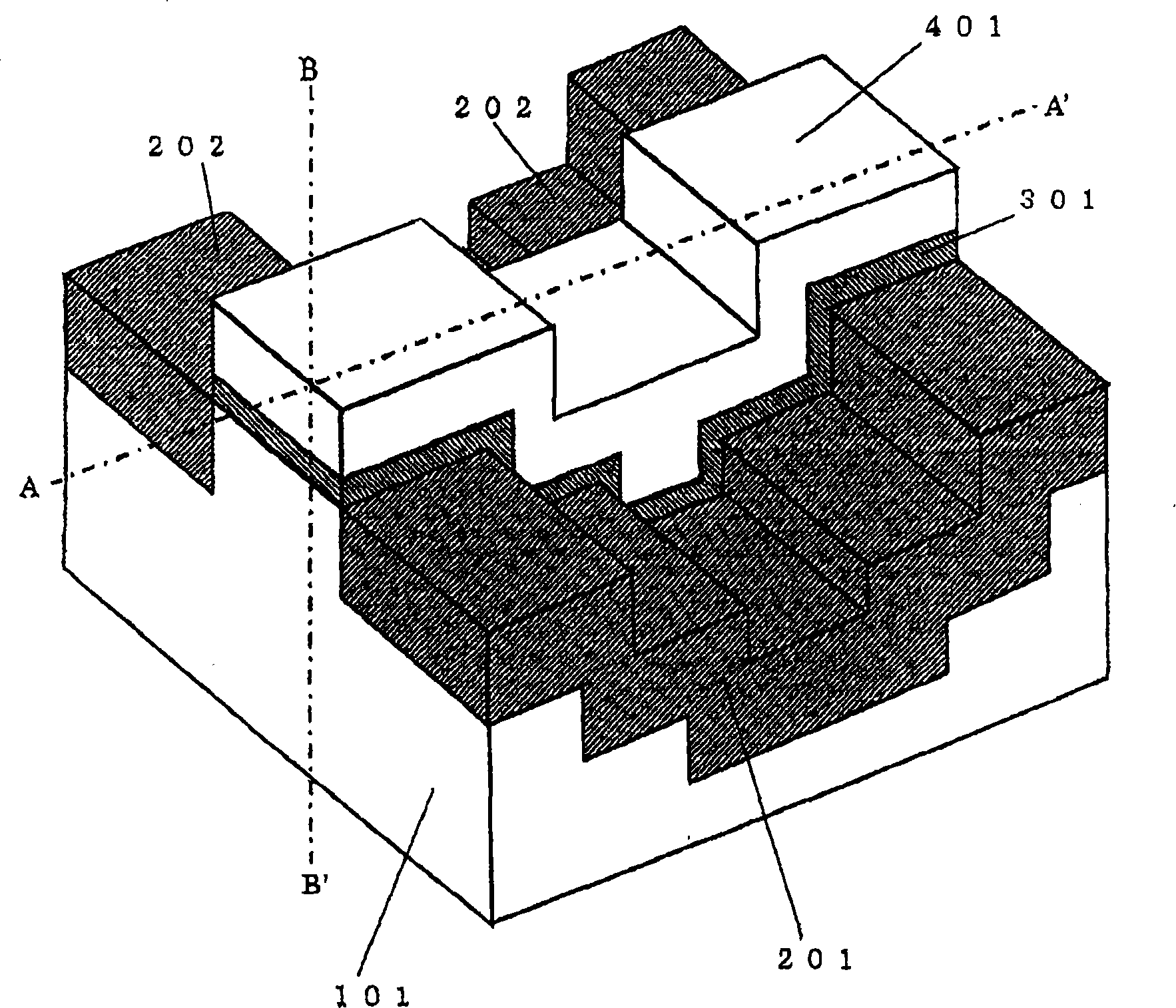
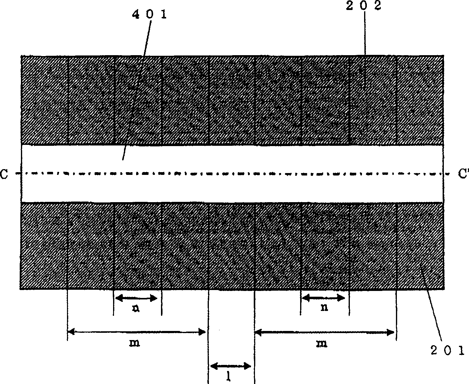
[0028] Figure 1 to Figure 4 A semiconductor device according to a first embodiment of the present invention is shown. figure 1 A lateral trench MOS transistor structure according to a first embodiment of the present invention is shown. figure 2 show includes figure 1 A cross-sectional view of the plane of the dashed-dotted line A-A' and the dashed-dotted line B-B'.
[0029] Such as figure 1 As shown, the n-type drain diffusion layer 201 and the n-type source diffusion layer 202 which become heavily doped impurity layers are formed on the p-type semiconductor substrate 101, and the gate insulating film 301 is formed on the p-type semiconductor substrate The substrate 101 is formed, and the gate electrode 401 is further formed on the gate insulating film 301 . In other words, the p-type semiconductor substrate 101, the n-type drain diffusion layer 201, the n-type source diffusion layer 202, and the gate electrode 401 serve as the substrate, drain, source, and gate of the...
no. 2 example
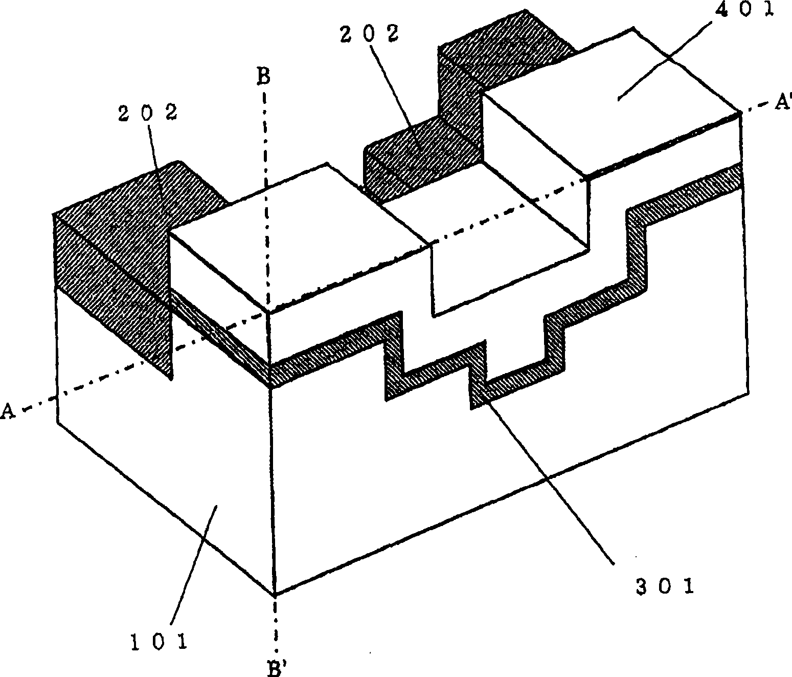
[0040] Figures 5 to 8 A semiconductor device according to a second embodiment of the present invention is shown. Figure 5 A lateral MOS transistor structure according to a second embodiment of the present invention is shown. Image 6 show includes Figure 5 Cross-sectional views of the planes of the dashed-dotted line D-D' and the dashed-dotted line E-E'.
[0041] Such as Figure 5 As shown, the n-type drain diffusion layer 201 and the n-type source diffusion layer 202 which become heavily doped impurity layers are formed on the p-type semiconductor substrate 101, and the gate insulating film 301 is formed on the p-type semiconductor substrate The substrate 101 is formed, and the gate electrode 401 is further formed on the gate insulating film 301 . The p-type semiconductor substrate 101, the n-type drain diffusion layer 201, the n-type source diffusion layer 202 and the gate electrode 401 are respectively used as the substrate, drain, source and gate of the MOS transist...
PUM
 Abstract
Description
Claims
Application Information