Red organic electroluminescent device and preparation thereof
A luminescent, red technology, applied in the field of red organic electroluminescent devices and their preparation, can solve the problems of incomplete energy transfer of trivalent europium complexes, unfavorable device luminous efficiency and brightness, only 1.4%, and achieve an increase in electroluminescence. Luminescent efficiency, increase carrier recombination probability, and weaken the effect of exciton concentration
- Summary
- Abstract
- Description
- Claims
- Application Information
AI Technical Summary
Problems solved by technology
Method used
Image
Examples
Embodiment 1
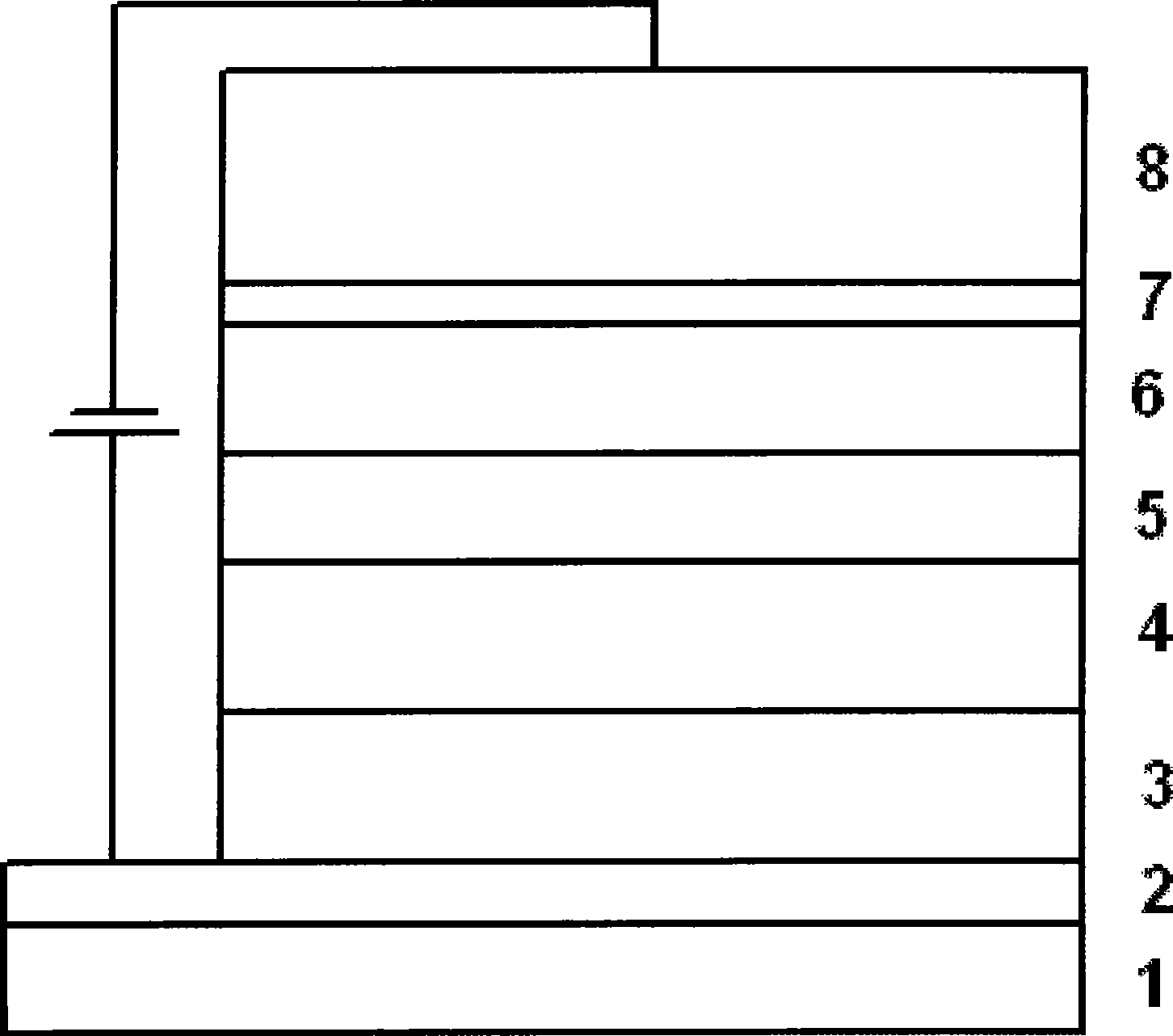
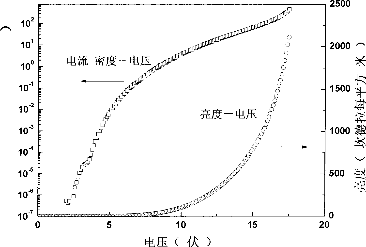
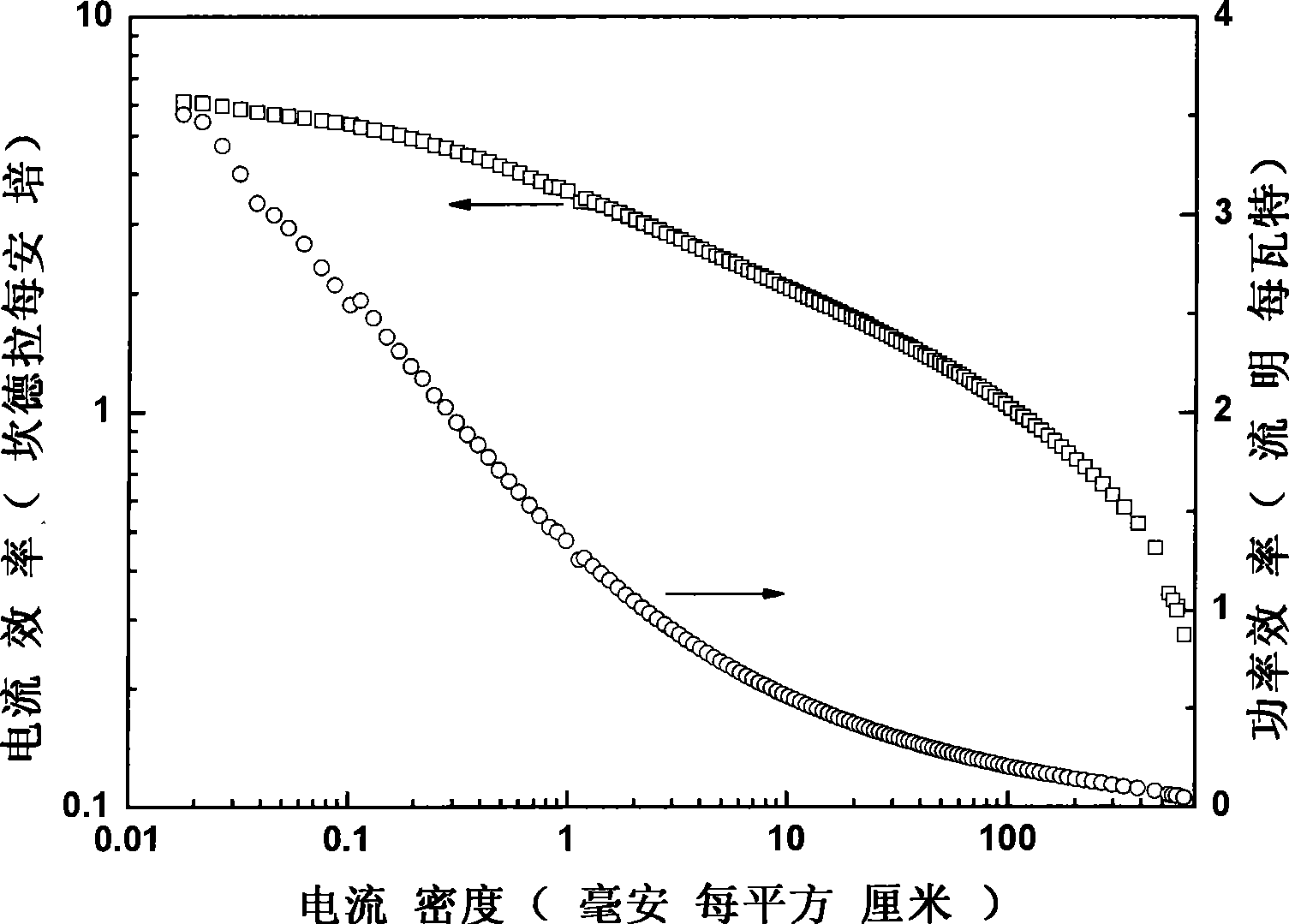
[0040] Firstly, the ITO anode layer on the ITO glass is chemically etched into strip electrodes with a width of 10 mm and a length of 30 mm, and then ultrasonically cleaned with cleaning solution and deionized water for 15 minutes and dried in an oven. Then put the dried substrate into the pretreatment vacuum chamber, and then transfer the ITO anode to the organic evaporation chamber after 10 minutes of low-pressure oxygen plasma treatment with a voltage of 250 volts under an atmosphere with a vacuum degree of 10 Pa. The vacuum degree is 1-5×10 -5 In Pa's organic evaporation chamber, a 50-nanometer-thick TPD hole-transport layer, a 45-nanometer-thick Eu(TTA) 3 The phen and AlQ were co-incorporated into the emitting layer of CBP, a 20-nm-thick BCP hole-blocking layer, and a 30-nm-thick AlQ electron-transporting layer. Next, the unfinished device is transferred to the metal evaporation chamber, in the 5-8×10 -5 A 1.0nm thick LiF buffer layer was evaporated sequentially under a...
Embodiment 2
[0042] Firstly, the ITO anode layer on the ITO glass is chemically etched into strip electrodes with a width of 10 mm and a length of 30 mm, and then ultrasonically cleaned with cleaning solution and deionized water for 15 minutes and dried in an oven. Then put the dried substrate into the pretreatment vacuum chamber, and then transfer the ITO anode to the organic evaporation chamber after 10 minutes of low-pressure oxygen plasma treatment with a voltage of 250 volts under an atmosphere with a vacuum degree of 10 Pa. The vacuum degree is 1-5×10 -5 In Pa's organic evaporation chamber, a 50-nanometer-thick TPD hole-transport layer, a 45-nanometer-thick Eu(TTA) 3 The phen and AlQ were co-incorporated into the emitting layer of CBP, a 20-nm-thick BCP hole-blocking layer, and a 30-nm-thick AlQ electron-transporting layer. Next, the unfinished device is transferred to the metal evaporation chamber, in the 5-8×10 -5 A 1.0nm thick LiF buffer layer was sequentially evaporated in a Pa...
Embodiment 3
[0044] Firstly, the ITO anode layer on the ITO glass is chemically etched into strip electrodes with a width of 10 mm and a length of 30 mm, and then ultrasonically cleaned with cleaning solution and deionized water for 15 minutes and dried in an oven. Then put the dried substrate into the pretreatment vacuum chamber, and then transfer the ITO anode to the organic evaporation chamber after 10 minutes of low-pressure oxygen plasma treatment with a voltage of 250 volts under an atmosphere with a vacuum degree of 10 Pa. The vacuum degree is 1-5×10 -5 In Pa's organic evaporation chamber, a 50-nanometer-thick TPD hole-transport layer, a 45-nanometer-thick Eu(TTA) 3 The phen and AlQ were co-incorporated into the emitting layer of CBP, a 20-nm-thick BCP hole-blocking layer, and a 30-nm-thick AlQ electron-transporting layer. Next, the unfinished device is transferred to the metal evaporation chamber, in the 5-8×10 -5 A 1.0 nm-thick LiF buffer layer was evaporated sequentially under ...
PUM
 Abstract
Description
Claims
Application Information


