

Method for making three-dimensional needlepoint electrode array based on parylene
A technology of electrode array and needle tip, which is applied in the production field of three-dimensional needle tip electrode array, can solve the problems of unfavorable high-density array chip structure design, low protrusion structure height, and inconspicuous protrusion effect, etc., to achieve effective current stimulation, Ease of control, reduction in area and power consumption
- Summary
- Abstract
- Description
- Claims
- Application Information
AI Technical Summary
Problems solved by technology
Method used
Image

Examples
Embodiment 1
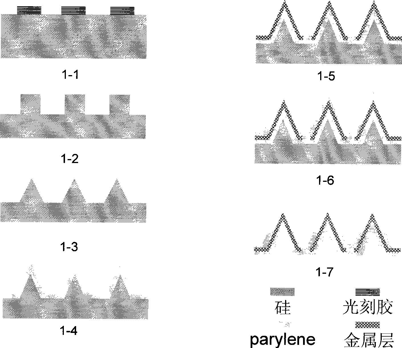
[0034] Example 1 figure 1 For the production process of the Parylene three-dimensional needlepoint electrode array according to the present invention is:
[0035] Step 1 attached Picture 1-1 , clean the silicon wafer, spin-coat a layer of ordinary positive photoresist with a thickness of about 10 μm on the silicon wafer and perform photolithography;
[0036] Step 2 attached Figure 1-2 , use an anisotropic ICP etching machine to etch silicon deeply to obtain silicon columns with a height of about 50 μm, and then remove the photoresist;
[0037] Step 3 attachedfigure 1 -3. Use isotropic HNA etching solution to modify the silicon columnar structure to form a silicon cone tip shape, and the obtained tip height is about 30 μm;
[0038] Step 4 attached figure 1 -4, Deposit a layer of Parylene film about 10 μm, as the substrate structure of the three-dimensional electrode array;
[0039] Step 5 Spin-coat a layer of AZ4620-type positive photoresist with a thickness of about 30 ...
Embodiment 2
[0043] Example 2 combined figure 1 and figure 2 The three-dimensional needle-tip electrode array based on Parylene has the characteristics of protrusions. The stimulation points of the electrodes are higher than the plane of the base material, and the uppermost part of the protrusions is in the shape of a needle tip, forming a Parylene-metallic sandwich structure similar to that shown in the figure. Layer-Parylene three-layer structure. The specific layout of the three-layer structure is as follows: first, a three-dimensional needle point array structure of silicon is etched out on the silicon substrate as a model of the three-dimensional structure of the Parylene flexible substrate, and a layer of Parylene film with good uniformity is covered on the silicon substrate The needle tip array structure of the transfer substrate is used as the substrate material of the final device; then, the needle tip electrodes and wires are formed on the Parylene by metal lift-off method; nex...
Embodiment 3
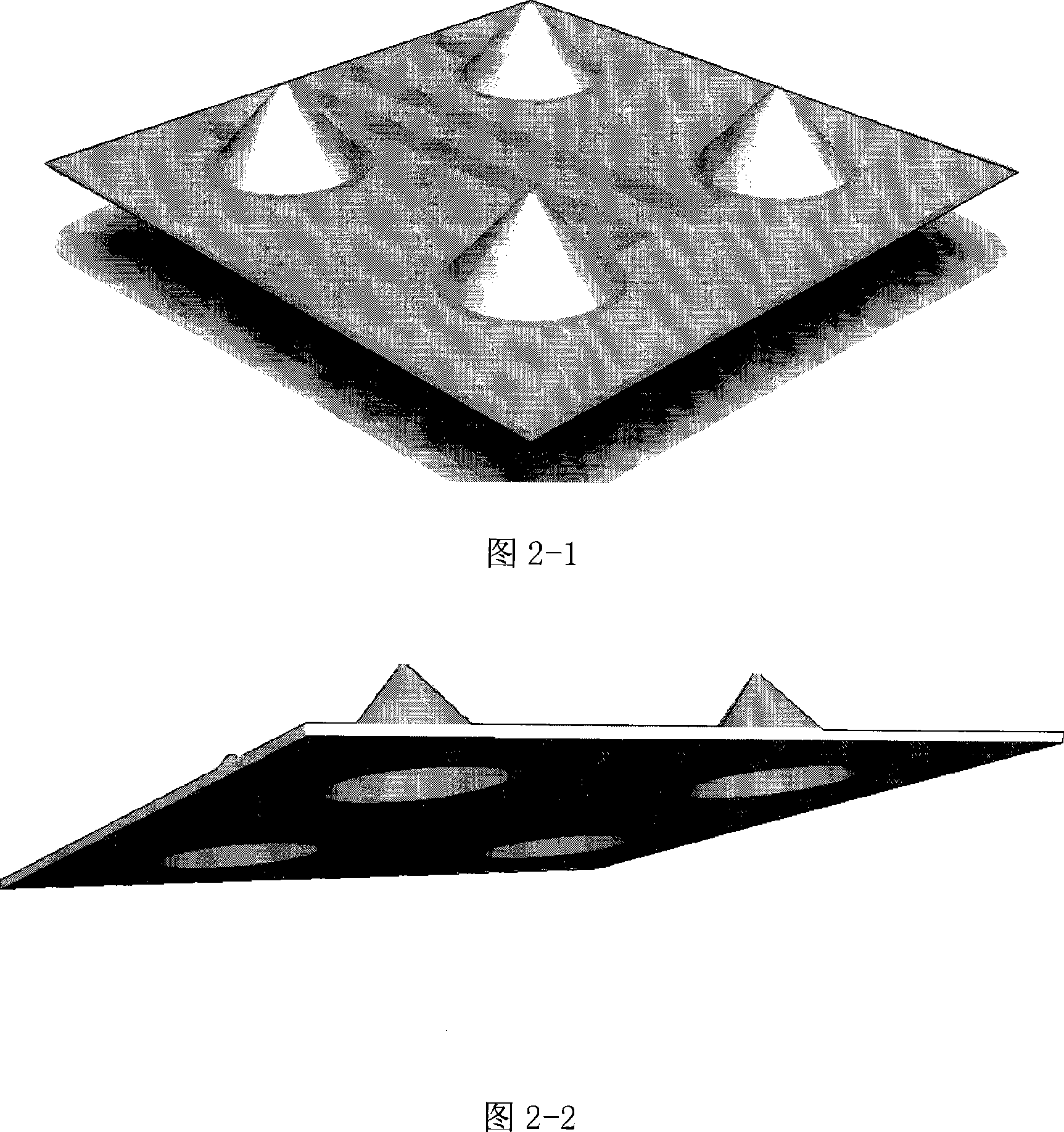
[0044] Example 3 figure 2 To ignore the Parylene three-dimensional tip electrode array morphology characteristics of the second layer of Parylene, where, diagram 2-1 It is a schematic diagram of the simulated morphology of the three-dimensional needle-tip electrode array, which is the effect of depositing metal and patterning; Figure 2-2 It is a schematic diagram of hollowing out the back cavity of the three-dimensional needle-point electrode of Parylene, in which the back side corresponding to the needle-point electrode of Parylene is hollow. This kind of silicon 3D needlepoint array structure produced by silicon substrate can be used as a model for subsequent Parylene transfer printing many times. As long as a qualified silicon 3D needlepoint array structure is produced, Parylene 3D needlepoint array structures with basically the same style can be produced in batches. Needle tip electrode array structure.
PUM
 Abstract
Description
Claims
Application Information