Chamber lining

A chamber and lining technology, applied in the field of microelectronics, can solve the problems of inability to effectively protect the pumping chamber, limit the uniformity of the flow field on the surface of the silicon wafer, and narrow the protection range, so as to improve the processing/processing quality, Large protection range and the effect of avoiding pollution

Active Publication Date: 2009-04-01
BEIJING NAURA MICROELECTRONICS EQUIP CO LTD
View PDF1 Cites 15 Cited by
  • Summary
  • Abstract
  • Description
  • Claims
  • Application Information

AI Technical Summary

Problems solved by technology

Second, the film can change the RF ground path and thus affect the quality of the processed device such as the obtained wafer
[0012] Although the lining described in the above Chinese patent can reduce or even avoid the formation of film accumulation on the inner wall of the processing chamber, thereby effectively protecting the inner wall of the processing chamber and reducing particle pollution , but it has the following defects: First, the range of protection of this lining structure is too narrow to effectively protect the adjustment bracket below the quartz window and the pumping chamber below the shielding plate, and cannot avoid the generation of particles to the greatest extent , thus causing contamination on the wafer; Second, the flow field in the processing chamber provided by this lining structure, especially the uniformity of the flow field on the surface of the silicon wafer, also has certain limitations, thus limiting the surface area of ​​the silicon wafer. The uniformity of the flow field is further improved; thirdly, and more importantly, the lining of this structure is only suitable for down-pumping or side-pumping semiconductor processing chambers, not for side-pumping semiconductor processing chambers

Method used


Image

  • Chamber lining
  • Chamber lining
  • Chamber lining

Examples


Embodiment Construction

[0030] In order to enable those skilled in the art to better understand the technical solution of the present invention, the lining of the chamber provided by the present invention will be described in detail below with reference to the accompanying drawings.

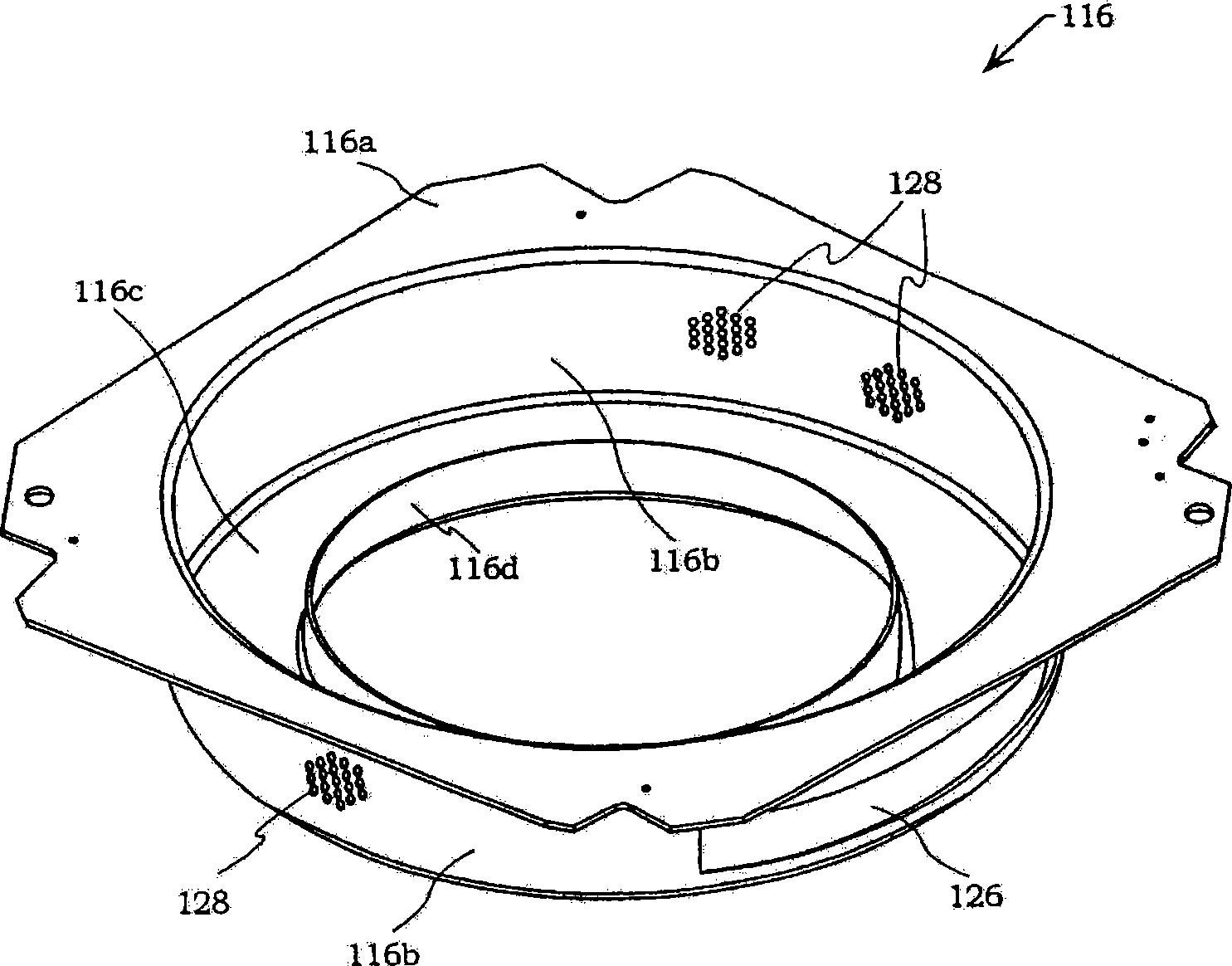
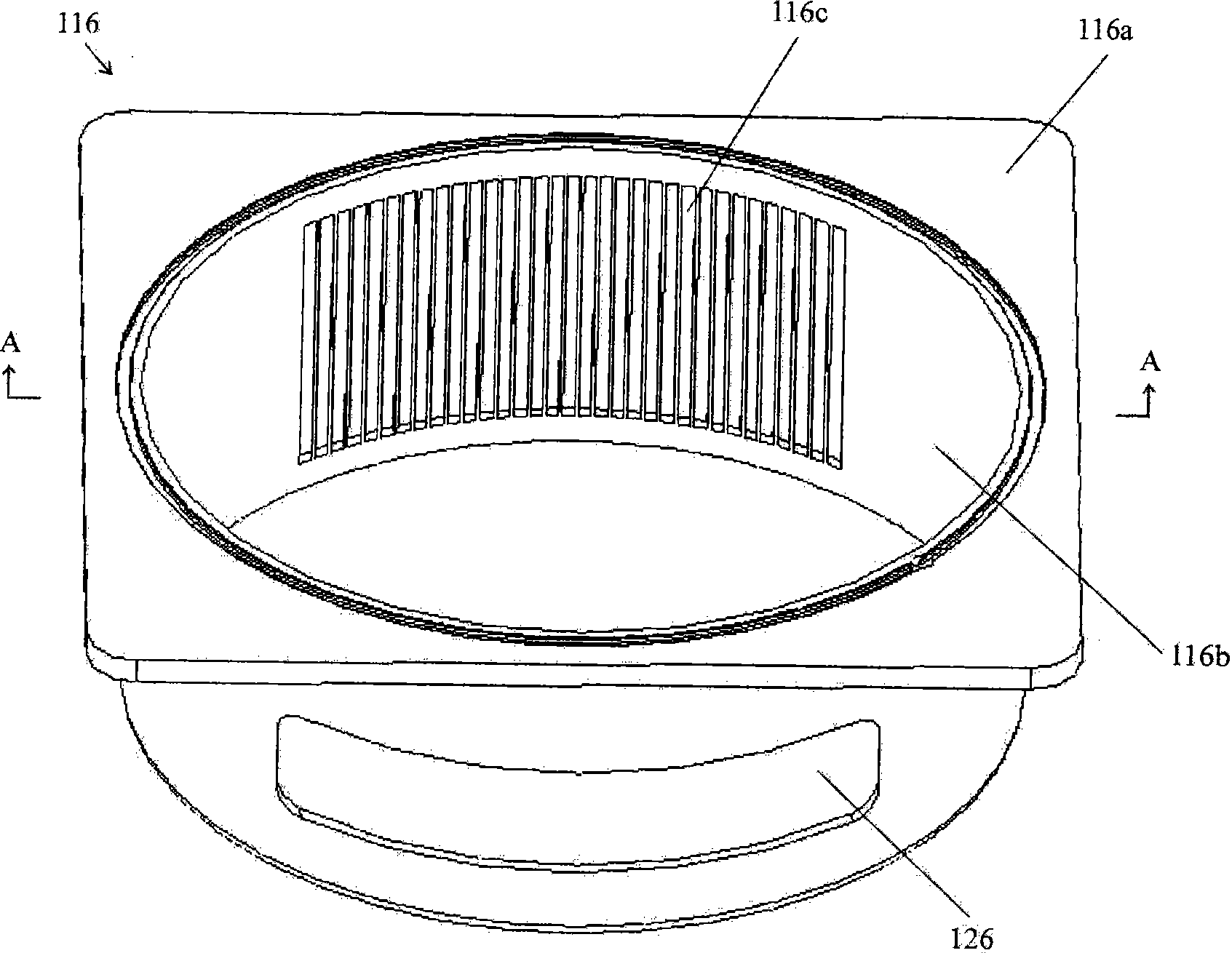
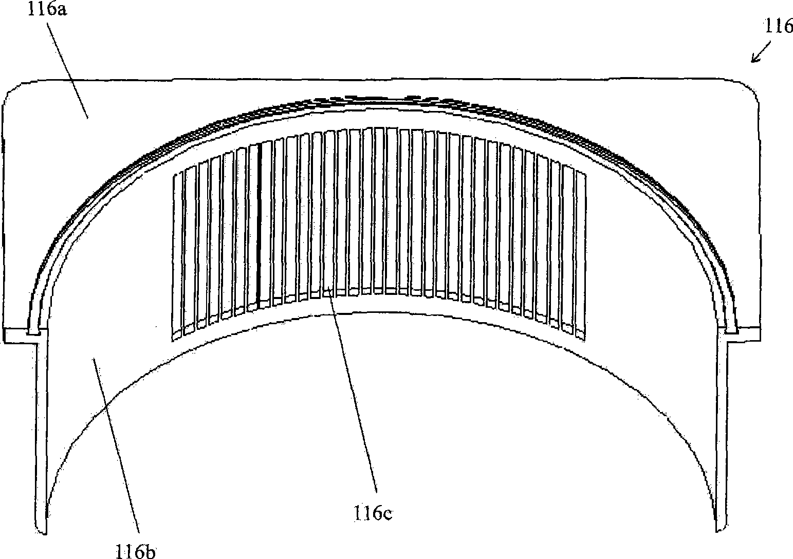
[0031] Please also see figure 2 and image 3 The liner 116 of the chamber provided by the first embodiment of the present invention includes a cylindrical outer wall 116b, an outer flange 116a extending outward from the upper edge of the outer wall 116b, a film delivery port 126 provided on the outer wall 116b, and A shielding hole 116c is opened at a position opposite to the film transfer port 126 on the outer wall 116b.

[0032] Wherein, the wafer transfer opening 126 is used as an entrance / exit for semiconductor devices such as wafers to enter / exit the processing chamber, and is arranged at a lower position on the outer side wall 116b.

[0033] The outer flange 116a is generally perpendicular to the outer sidewall...


PUM


Abstract

The invention provides a chamber liner which is used for lining in a semiconductor chamber. The liner comprises a side wall, the shape and the size of which match with those of the inner wall of the semiconductor chamber, and the side wall of the liner is provided with a shield pore. The chamber liner provided by the invention is suitable for the side pulling semiconductor chamber, and film accumulation generated on the inner wall of the chamber can be reduced or even avoided, thus protecting the inner wall of the chamber effectively, reducing particle contamination and further improving the processing / treating quality of semiconductor devices, wafer, etc.

Description

technical field [0001] The invention relates to the technical field of microelectronics, in particular, to a lining for chambers in semiconductor processing / processing techniques. Background technique [0002] As we all know, semiconductor manufacturing technology includes processes such as deposition of metals, dielectrics, and other semiconductor materials, etching of the above materials, and removal of photoresist mask layers. Wherein, the etching process includes gate etching, dielectric etching, metal etching, etc., and plasma etching technology is widely used in these etching processes. [0003] The above-mentioned semiconductor manufacturing and processing processes usually need to be performed in a semiconductor processing chamber. A typical semiconductor processing chamber includes a chamber, plasma generation and control equipment, process gas delivery equipment, wafer chucks for wafer holding, and process components. Among them, the process components are used t...

Claims


Application Information

Patent Timeline
Patent Type & Authority Applications(China)
IPC IPC(8): H01L21/3065C23F1/08
Inventor 林盛
Owner BEIJING NAURA MICROELECTRONICS EQUIP CO LTD
Why Eureka
Try Eureka