Method of manufacturing metal doping ZnO film

A metal doping and thin film technology, applied in metal material coating process, ion implantation plating, coating and other directions, can solve the problems of complex preparation process of MZO thin film, not easy to control and adjust, and many research and development processes, etc. The effect of the overall R&D process, the continuous stability of sputtering, and the optimization of optical and electrical properties

Inactive Publication Date: 2009-04-08
SHANGHAI UNIV OF ENG SCI
View PDF0 Cites 9 Cited by
  • Summary
  • Abstract
  • Description
  • Claims
  • Application Information

AI Technical Summary

Problems solved by technology

In addition, the current MZO thin film preparation process is also very complicated, it is not easy to control an

Method used


Image

  • Method of manufacturing metal doping ZnO film
  • Method of manufacturing metal doping ZnO film
  • Method of manufacturing metal doping ZnO film

Examples


Embodiment 1

[0028] Embodiment one: prepare Al metal doped ZnO film, its step is:

[0029] (1) Substrate cleaning: take the glass substrate, clean it and put it on the sample holder of the radio frequency magnetron sputtering chamber, place the substrate to be deposited facing down, effectively avoiding contamination of the substrate by impurities.

[0030] (2) Extraction of high vacuum: the vacuum degree of the sputtering chamber is evacuated to 2×10 -4 Pa for high cleanliness vacuum.

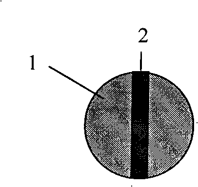
[0031] (3) Adjusting the metal and its doping amount: take two Al metal strips and fix them on the Zn target, and the fixing method of the metal strips is symmetrical and radial at the center of the circle. The area ratio of the used metal strips to the Zn target can be measured and calculated. Combined with the different sputtering yields under the same conditions, the doping amount of metal in the ZnO film can be determined, and the metal doping amount of the metal-doped ZnO film can be determined. Imp...

Embodiment 2

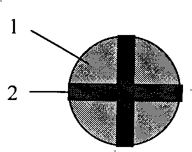
[0035] Embodiment two: (1), (2), (4) (5) (6) remain unchanged in the whole film preparation process of embodiment one, only change (3) adjust the number of Al metal strips, get 4 pieces of Al The metal strip is fixed on the Zn target in a symmetrical radial manner. In this way, thin films with different metal doping levels can be obtained.

Embodiment 3

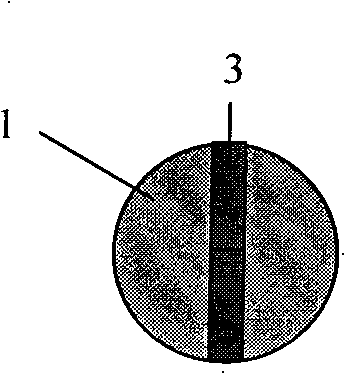
[0036] Embodiment three: (1), (2), (4) (5) (6) remain unchanged in the whole thin film preparation process of example one, only change (3) change metal strip, get 2 Ag metal strips and fix On the Zn target, the fixing method is symmetrical and radial. In this way, Ag metal-doped ZnO films can be obtained.


PUM


Abstract

The invention relates to the field of semiconductor materials, in particular to a method for preparing a metal film doped with ZnO. The method is characterized by comprising the following steps: a substrate is arranged in a magnetron sputtering room after being cleaned and a reaction room thereof is pumped to vacuum with high cleanliness; high-purity metal strips are taken as adulterants and high-purity Zn are taken as materials, and metal strips are fixed on a Zn target according to a plurality of proportions; pure Ar gas and pure oxygen are taken as sputtering gas and reaction gas to be input into the vacuum reaction sputtering room by the control of a flowmeter for sputtering growth; and annealing treatment is carried out in vacuum environment after growth. The invention has the following beneficial effects: the control of metal doping content is realized, and the effect of oxidation on the metal target during the reaction sputtering is effectively reduced by the pattern of radio frequency sputtering during the reaction, thus leading the sputtering to keep continuous and stable; and finally, by being combined with the corresponding vacuum annealing technology, the optical and electrical properties of the MZO film are optimized. The preparation method simplifies technical processes, reduces the whole development procedure, shortens the period and saves the cost.

Description

[technical field] [0001] The invention relates to the technical field of semiconductor materials, in particular to a method for preparing a metal-doped ZnO thin film. [Background technique] [0002] Transparent conductive electrodes are required in optical devices such as solar cells and flat panel displays, which is the main application field of transparent conductive films. The transparent conductive film needs to have the following properties: 1. High transmittance to visible light (its wavelength covers 380 to 780nm), with an average light transmittance greater than 80%; 2. Good electrical conductivity, with a resistivity of 10 -2 Ω·cm or less. Among them, being transparent in the visible light band means that the energy bandgap width of the material is large (Eg is greater than 3eV), which determines that there are few carriers in its conduction band or valence band. On the other hand, metal materials with high electrical conductivity often have more carriers, but bec...

Claims


Application Information

Patent Timeline
IPC IPC(8): C23C14/35C23C14/08C23C14/58
Inventor 言智张恩霞周细应何佳于治水
Owner SHANGHAI UNIV OF ENG SCI
Why Eureka
Try Eureka