Current mirror type TFT-OLED display image element unit circuit and its production method

A technology of TFT-OLED and display pixels, which is applied in the field of thin-film microelectronic circuit design and device preparation, can solve problems such as uneven display brightness of the display screen, and achieve the effect of improving image response speed, consistency and accuracy

Inactive Publication Date: 2009-04-08
NANKAI UNIV
View PDF3 Cites 18 Cited by
  • Summary
  • Abstract
  • Description
  • Claims
  • Application Information

AI Technical Summary

Problems solved by technology

[0002] Organic Light Emitting Diode (OLED) is a new display device with great potential (A Novel Technique to Study OLED Function Marc Sims, Steven W. Venter and Ian D. Parker SID 08 Digest page 223), OLED uses current For driving, the traditional driving method is to use two tubes of thin film field effect transistors (Thin Film Transistor, TFT) to drive, for example, the Chinese patent application number is CN200710056020. Manufacturing method of polysilicon TFT array in light-emitting display screen", however, this kind of circuit that uses two TFT tubes to drive often has the disadvantage of uneven display brightness of the display screen

Method used


Image

  • Current mirror type TFT-OLED display image element unit circuit and its production method
  • Current mirror type TFT-OLED display image element unit circuit and its production method
  • Current mirror type TFT-OLED display image element unit circuit and its production method

Examples


preparation example Construction

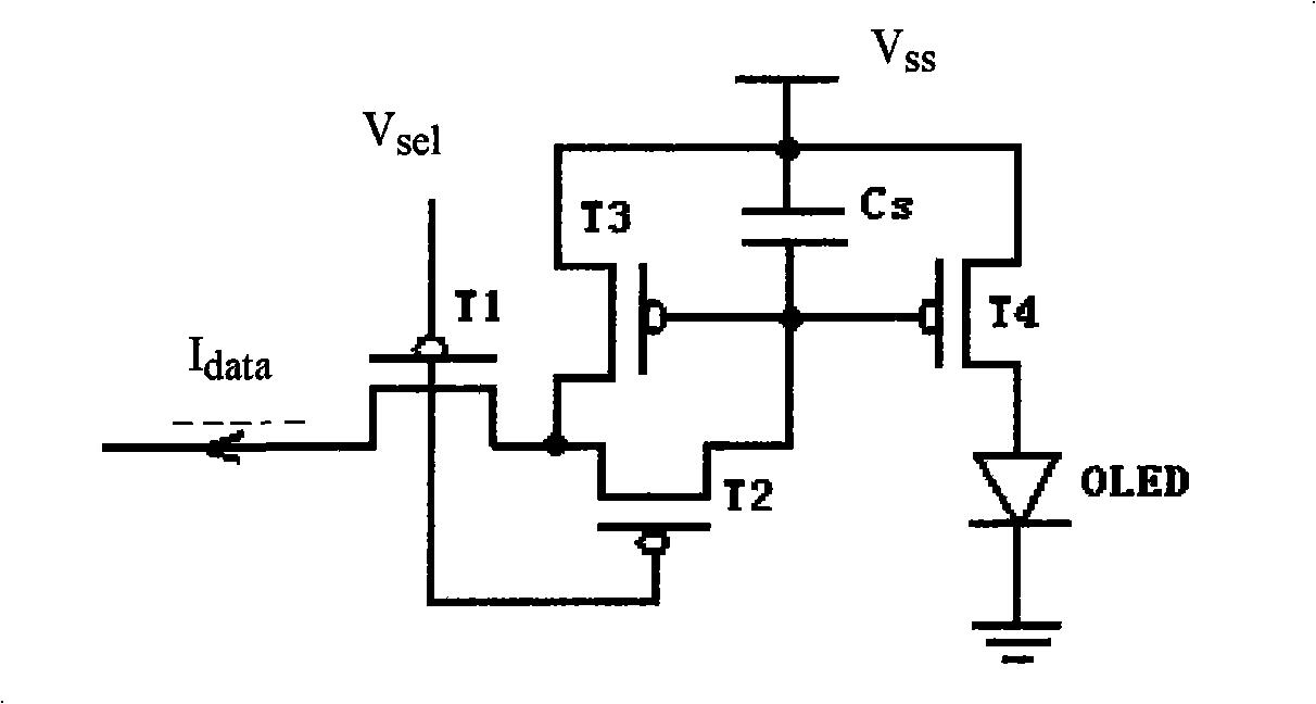
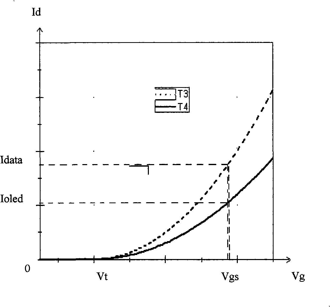
[0071] The invention provides a method for preparing a high-performance polysilicon thin film transistor current mirror by adopting a method of metal-induced single-direction lateral crystallization or laser crystallization. Use amorphous silicon metal to induce single-direction lateral crystallization or laser crystallization to form polysilicon islands on the dehydrogenated amorphous silicon film, and select the crystallization intervals in the polysilicon islands in parallel as the channels of mirror transistors T3 and T4 respectively Area, forming a specific high-quality polysilicon TFT tube layout. Compared with the conventional current mirror, the device carrier mobility, threshold voltage, gate capacitance and sub-threshold swing of the two mirror tubes prepared by the present invention are very close, and the ratio of the mirror current depends on the ratio of the two TFTs more accurately. The ratio of width to length.

[0072] In the present invention, the conduction...

specific Embodiment approach 1

[0100] The invention provides a method for preparing lateral crystallization of a thin film field effect transistor TFT in a current mirror type TFT-OLED display pixel unit circuit. The method adopts a metal-induced single-direction lateral crystallization technology.

[0101] Such as image 3 As shown, the present invention is on a transparent glass substrate, on a polysilicon island prepared by metal-induced unidirectional lateral crystallization, according to the method for constructing a current mirror with the above-mentioned thin film transistor, the method ensures that the device has the same characteristics as conventional MIUC polysilicon TFT On the basis of the excellent performance of the current mirror, the specific position of the two mirror tubes is set by using a specific current mirror layout design, which obviously improves the mirror image characteristics of the current mirror.

[0102] Such as Figure 4 , Figure 5 As shown, the substrate material for prep...

specific Embodiment approach 2

[0110] The invention also provides a laser crystallization preparation method of a thin film field effect transistor TFT in a current mirror type TFT-OLED display pixel unit circuit, and the method adopts a laser crystallization technology.

[0111] The present invention is a method for constructing a current mirror by preparing a laser crystallized thin film transistor on a polysilicon island on a transparent glass substrate. The mirror layout design sets the specific positions of the two mirror tubes in the laser crystallization process, which significantly improves the mirror image characteristics of the current mirror.

[0112] Such as Figure 18 As shown, the substrate material for preparing polysilicon devices is transparent substrate glass 201. In order to block impurities in the glass substrate, they diffuse into the active layer during the thermal process of device preparation, and deposit silicon nitride on the glass substrate and LTO hybrid layer 202 . The precurs...


PUM


Abstract

The present invention discloses a current mirror type TFT-OLED display pixel unit circuit, which comprises four polysilicon TFT tubes T1, T2, T3 and T4, an organic light emitting diode (OLED) and a capacitor Cs, wherein, the tubes T3 and T4 are completely symmetrical and form a current mirror; the tubes T1 and T2 serve as switch tubes, and line scanning signals are put in the grids of the tubes T1 and T2 to control the on-off of data current; the capacitor Cs is used for storing display data in a voltage mode, and the voltage on both ends of the capacitor Cs is loaded to the grid of the tube T4 to drive OLED to emit light; and the polysilicon TFT tubes T1, T2, T3 and T4 are all P channel devices. The present invention also provides a preparation method for transversal crystallization or laser crystallization of a mirror image TFT tube with high quality. The current mirror type TFT-OLED display pixel unit circuit and the method of the invention can enhance the consistency and precision of device properties of the TFT tube which forms mirror image current and can improve the image response speed, the image gray level and the picture display quality of an OLED screen.

Description

technical field [0001] The invention relates to thin-film microelectronic circuit design and device preparation technology, in particular to a current mirror type TFT-OLED display pixel unit circuit and a preparation method. The invention adopts metal-induced single-direction lateral crystallization or laser crystallization technology to form high-quality polysilicon islands on dehydrogenated amorphous silicon films, and then selects specific interval positions on the polysilicon islands to form a pair of films in parallel arrangement. Transistors, so as to obtain the technology of a current mirror composed of a pair of thin film field effect transistors with relatively consistent material characteristics. Background technique [0002] Organic Light Emitting Diode (OLED) is a new display device with great potential (A Novel Technique to Study OLED Function Marc Sims, Steven W. Venter and Ian D. Parker SID 08 Digest page 223), OLED uses current For driving, the traditional d...

Claims


Application Information

Patent Timeline
Patent Type & Authority Applications(China)
IPC IPC(8): G09G3/32H01L27/32H01L21/84H01L21/336H01L21/20G09G3/3241
Inventor 孟志国孙鹏飞李娟吴春亚熊绍珍
Owner NANKAI UNIV
Why Eureka
Try Eureka