Non-gap bonding course GaN based illuminating device and its production method

A light-emitting device, seamless technology, applied in semiconductor devices, electrical components, circuits, etc., can solve problems such as poor bonding between GaN-based light-emitting devices and supporting components, reduce the incidence of cracks, help heat dissipation, improve The effect of yield

Active Publication Date: 2009-04-08
XIAMEN SANAN OPTOELECTRONICS TECH CO LTD
View PDF0 Cites 12 Cited by
  • Summary
  • Abstract
  • Description
  • Claims
  • Application Information

AI Technical Summary

Problems solved by technology

[0003] In order to solve the problem of poor bonding between the above-mentioned GaN-based light-emitting device and the supporting part, and improve the yield after laser lift-off, the present invention aims to propose a GaN-based light-emitting device with a seamless bonding process and its preparation method

Method used


Image

  • Non-gap bonding course GaN based illuminating device and its production method
  • Non-gap bonding course GaN based illuminating device and its production method
  • Non-gap bonding course GaN based illuminating device and its production method

Examples


Embodiment Construction

[0022] The present invention will be further described below in conjunction with the accompanying drawings and embodiments.

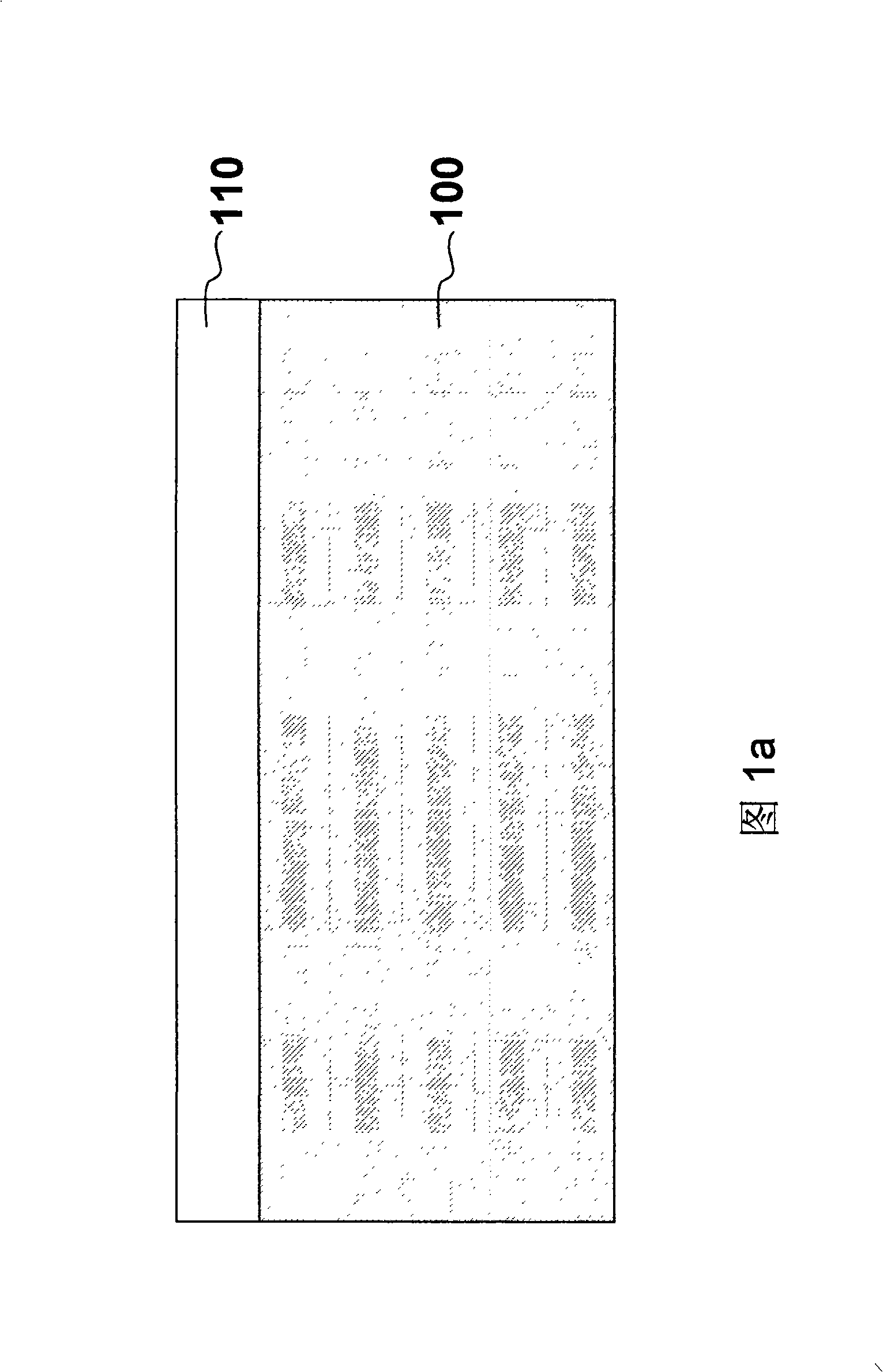
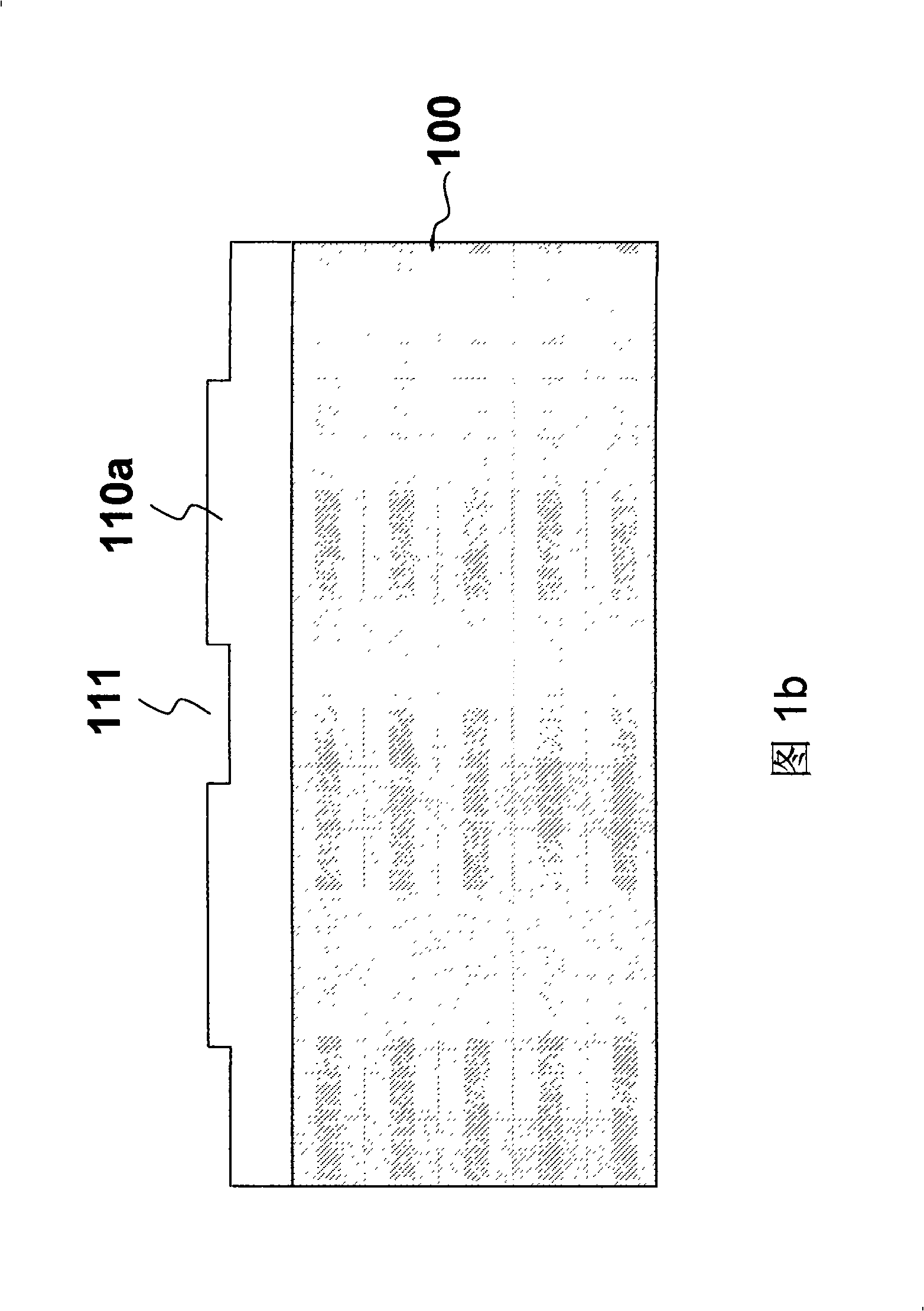
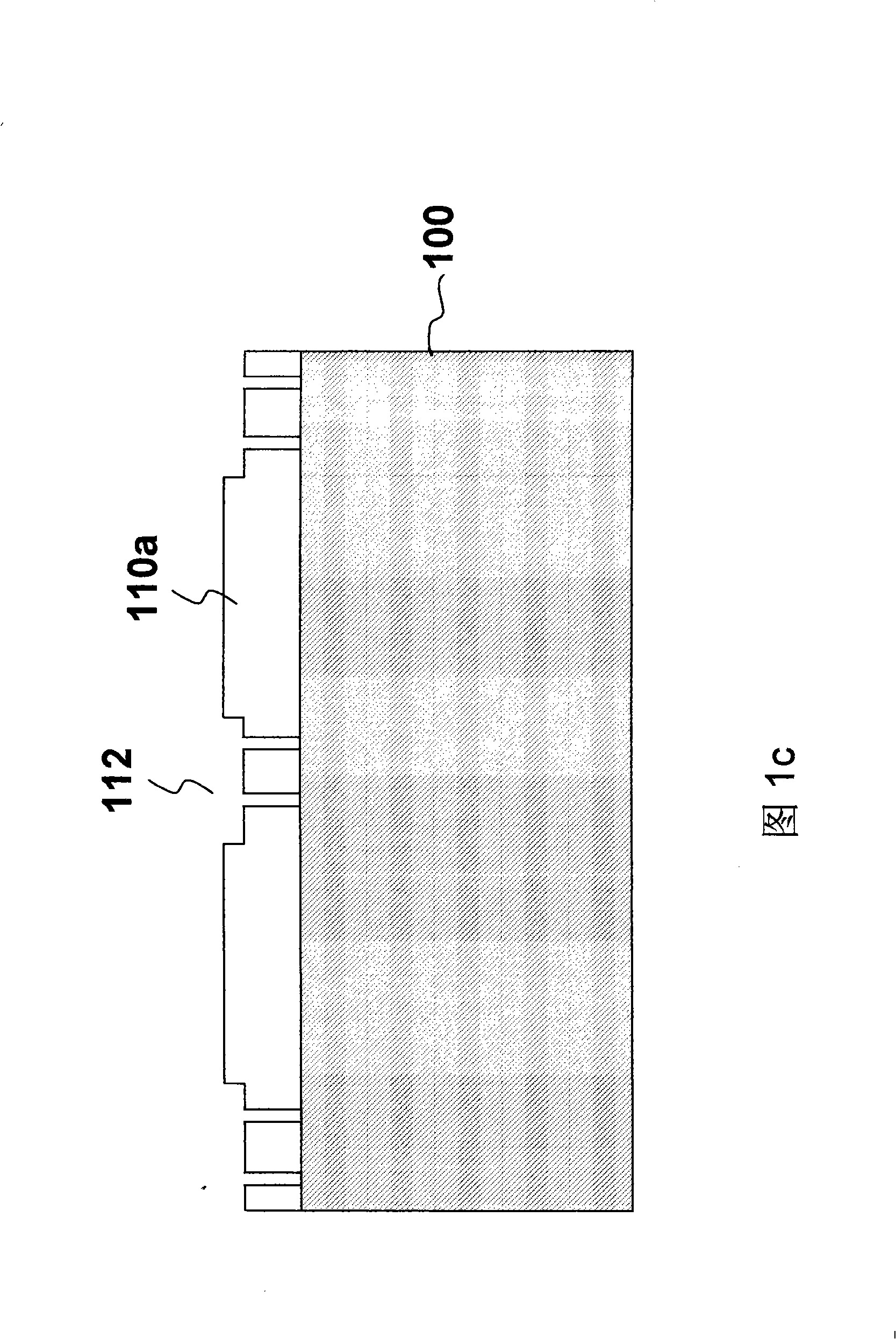
[0023] A GaN-based light-emitting device with a seamless bonding process as shown in Figure 2, including a GaN-based epitaxial film 110 with an N semiconductor layer, an active layer and a P semiconductor layer; an ohmic contact and a metal reflective layer are formed under the P semiconductor layer 120, the reflective metal film material is preferably Ag, with a thickness of 50-500nm; a multilayer metal film 150 is formed under the reflective metal film; a eutectic solder layer 160 is formed on the multilayer metal film 150; the eutectic solder layer 160 is connected with the support The component 200 is bonded; the N electrode 170 material layer is formed on the N semiconductor layer; the P electrode 210 material layer is formed at the bottom of the supporting component; the side wall of the GaN-based light-emitting device of the present invention wrap...


PUM


Abstract

The invention discloses a GaN-based light emitting device for a gapless bonding process and a preparation method thereof. Absolute separation among GaN-based unit light emitting devices is realized by removing part of GaN epitaxial layers by dry etching and gashing the GaN epitaxial layers by laser; a passive film wraps side wall of the light emitting device to ensure the absolute electrical disconnection between the device and a depth compensation film; by depositing the depth compensation film in a groove formed in the mutually separated unit GaN-based light emitting devices, the deposition depth is flush with table tops at two sides to form a plane with same height, thus realizing the gapless bonding between the GaN-based light emitting devices and a support part, reducing the crack rate in the laser stripping course and enhancing the yield; and the depth compensation film is a metal material with high reflectivity and is reserved on the side wall part of the light emitting devices, thereby reducing the light loss of the side wall of the light emitting devices and improving the light emitting efficiency of the devices, and being helpful to heat emission of the devices.

Description

technical field [0001] The invention relates to a GaN-based semiconductor optoelectronic device, in particular to a GaN-based light-emitting device with a seamless bonding process and a preparation method thereof. Background technique [0002] At present, most GaN-based epitaxy is mainly grown on sapphire substrates. Due to the poor conductivity of sapphire, ordinary GaN-based light-emitting devices adopt a lateral structure, that is, the two electrodes are on the same side of the device, and the current flows laterally in the N-GaN layer. The distance is not equal, and there is a problem of current blockage and heat generation; in addition, the thermal conductivity of the sapphire substrate is low, which limits the luminous power and efficiency of GaN-based devices; removing sapphire and making the light-emitting device into a vertical structure can effectively solve heat dissipation , light emission, and antistatic issues. At present, the laser lift-off sapphire substrate ...

Claims


Application Information

Patent Timeline
Patent Type & Authority Applications(China)
IPC IPC(8): H01L33/00
Inventor 林雪娇潘群峰洪灵愿陈文欣吴志强
Owner XIAMEN SANAN OPTOELECTRONICS TECH CO LTD
Why Eureka
Try Eureka