
Splicing PCB board produced by paper fiber sheet material

A technology for making PCB boards and plates, which is applied in the direction of assembling printed circuits and printed circuit components with electrical components, which can solve problems such as breaking, failure, and fiber length, and achieve the effect of avoiding cracks and reducing the effect of thermal expansion and contraction.

Inactive Publication Date: 2009-04-08
佛山市顺德区骏达电子有限公司
View PDF0 Cites 0 Cited by
  • Summary
  • Abstract
  • Description
  • Claims
  • Application Information

AI Technical Summary

Problems solved by technology

In order to reduce production costs, splicing PCB boards made of multiple paper fiber sheets are now used instead of splicing PCB boards made of expensive epoxy glass fiber sheets. The combined area of ​​the board is large and the fibers are long. Under the effect of thermal expansion and contraction, the paper fibers of the PCB board will be broken by stress, resulting in cracks and failure, causing the PCB board to be scrapped.

Method used


Image

  • Splicing PCB board produced by paper fiber sheet material
  • Splicing PCB board produced by paper fiber sheet material
  • Splicing PCB board produced by paper fiber sheet material

Examples


Embodiment approach

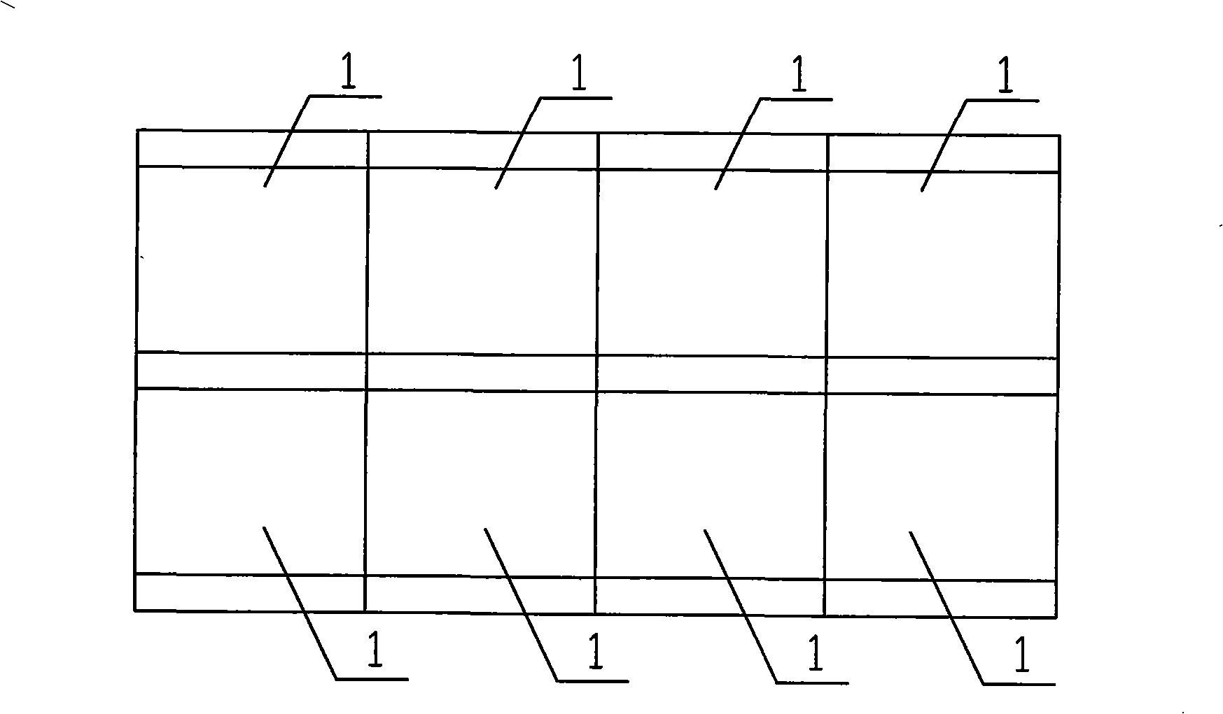
[0015] Implementation method: figure 1 Shown is a schematic structural diagram of a spliced ​​PCB board made of paper fiber boards in the prior art. It is mainly composed of multiple PCB units 1 spliced ​​into a whole PCB board. Each PCB unit 1 is assembled with zero spacing, and " V" shaped pit. If the spliced ​​PCB board with this structure has a large area, the spliced ​​PCB board will undergo physical changes in thermal expansion and contraction during the high-temperature reflow soldering process, which will cause cracks in the spliced ​​PCB board and cause the product to be scrapped.

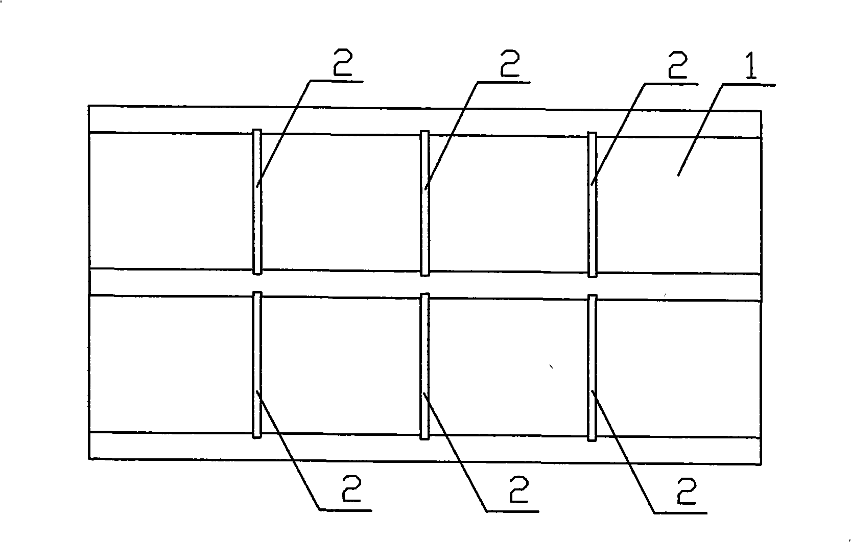
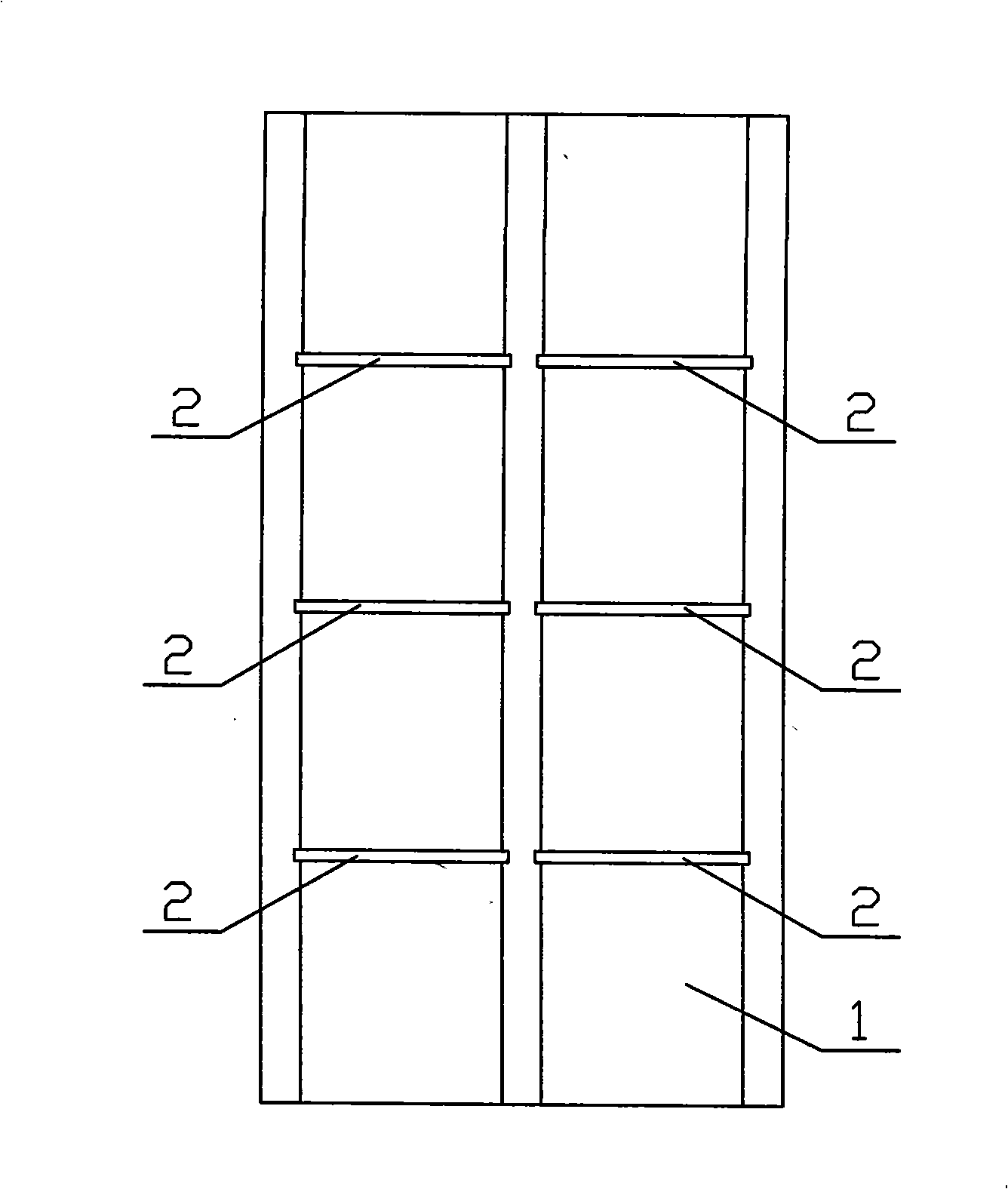
[0016] In order to overcome this problem, the present invention improves the structure of the spliced ​​PCB board made of paper fiber board. like figure 2 As shown, a plurality of PCB units 1 are spliced ​​into a whole PCB board, and there are two rows and three rows of six elongated slots 2 in the longitudinal direction on the spliced ​​PCB board. The fiber length of the board is chan...


PUM


Abstract

The invention relates to a splice Printed Circuit Board (PCB) made from paper fibre plates, which is capable of preventing cracks from forming in the process of the Surface Mounting Technology (SMT). The splice PCB consists of a PCB which is formed by splicing a plurality of PCB units into a whole. The splice PCB is characterised in that the splice PCB is opened with strip-shaped grooves. Two or more strip-shaped grooves are arranged and the strip-shaped grooves are evenly distributed on the splice PCB. The strip-shaped grooves are evenly distributed on the splice PCB along the horizontal direction. The strip-shaped grooves are evenly distributed on the splice PCB along the vertical direction. The strip-shaped grooves are evenly distributed on the splice PCB, combining horizontal and vertical distributions. The splice PCB adopting the structure is effective for preventing cracks from forming in the SMT process, thereby improving product percent of pass.

Description

technical field [0001] The invention relates to a spliced ​​PCB board made of paper fiber boards which prevents cracks in the SMT process. Background technique [0002] Chip reflow soldering (SMT) is a soldering installation process developed to adapt to the new high-density mounting. In the SMT process, the PCB has undergone an alternating process of room temperature → preheating → 230°C high-temperature reflow soldering → random cooling → room temperature, and the substrate of the PCB also simultaneously undergoes "thermal expansion and contraction". At present, the SMT process design generally uses expensive epoxy glass fiber boards to make circuit boards (PCB boards) to overcome the thermal shock of the SMT process on the PCB during high-temperature reflow soldering. Especially in recent years, countries around the world have attached great importance to environmental protection, and have implemented restrictions on the use of lead-containing tin, and the flow temperatu...

Claims


Application Information

Patent Timeline
Patent Type & Authority Applications(China)
IPC IPC(8): H05K1/02H05K3/34
Inventor 蔡江
Owner 佛山市顺德区骏达电子有限公司
Learn More