Thin-film transistor and LCD device

A technology of liquid crystal display device and thin film transistor, which is applied to transistors, electric solid devices, semiconductor devices, etc., can solve the problems of affecting the writing voltage, excessive writing resistance, sudden change of pixel voltage, etc., so as to improve the display quality and reduce the Small parasitic capacitance, reduced width effect

Inactive Publication Date: 2009-05-06
SHANGHAI SVA LIQUID CRYSTAL DISPLAY
View PDF0 Cites 5 Cited by
  • Summary
  • Abstract
  • Description
  • Claims
  • Application Information

AI Technical Summary

Problems solved by technology

Due to the influence of TFT characteristic changes caused by deviations in the exposure and etching processes, the pixel voltage will change suddenly, and the center of the positive and negative write voltages deviates from the original com voltage, resulting in flickering during display
[0007] In addition, the instability of the process leads to changes in the overlapping area between the source, drain and gate, which will cause problems such as excessive write resistance, which will affect the final write voltage.

Method used


Image

  • Thin-film transistor and LCD device
  • Thin-film transistor and LCD device
  • Thin-film transistor and LCD device

Examples


Embodiment Construction

[0018] The thin film transistor and the liquid crystal display device of the present invention will be further described in detail below with reference to the accompanying drawings.

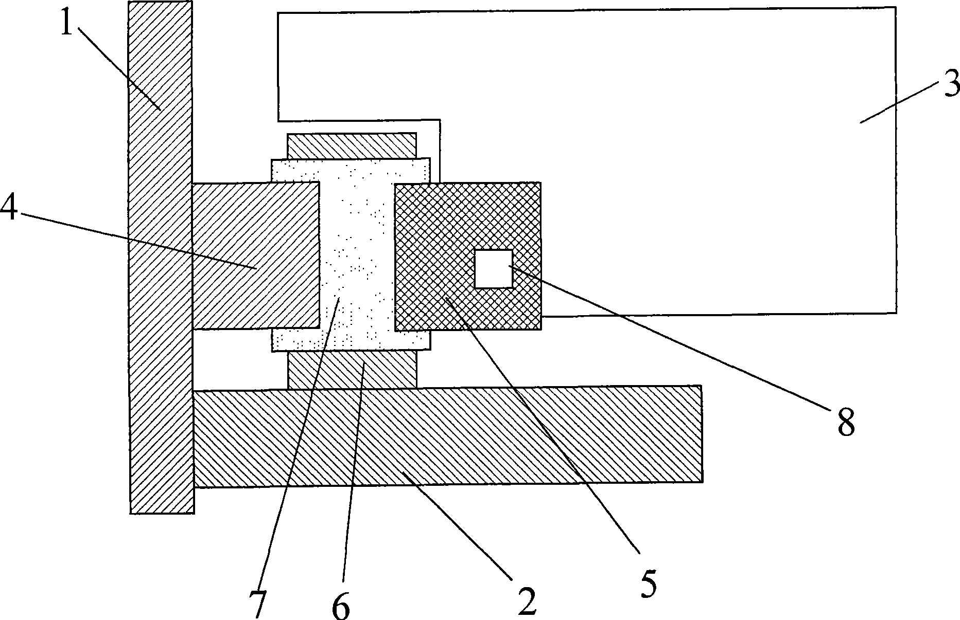
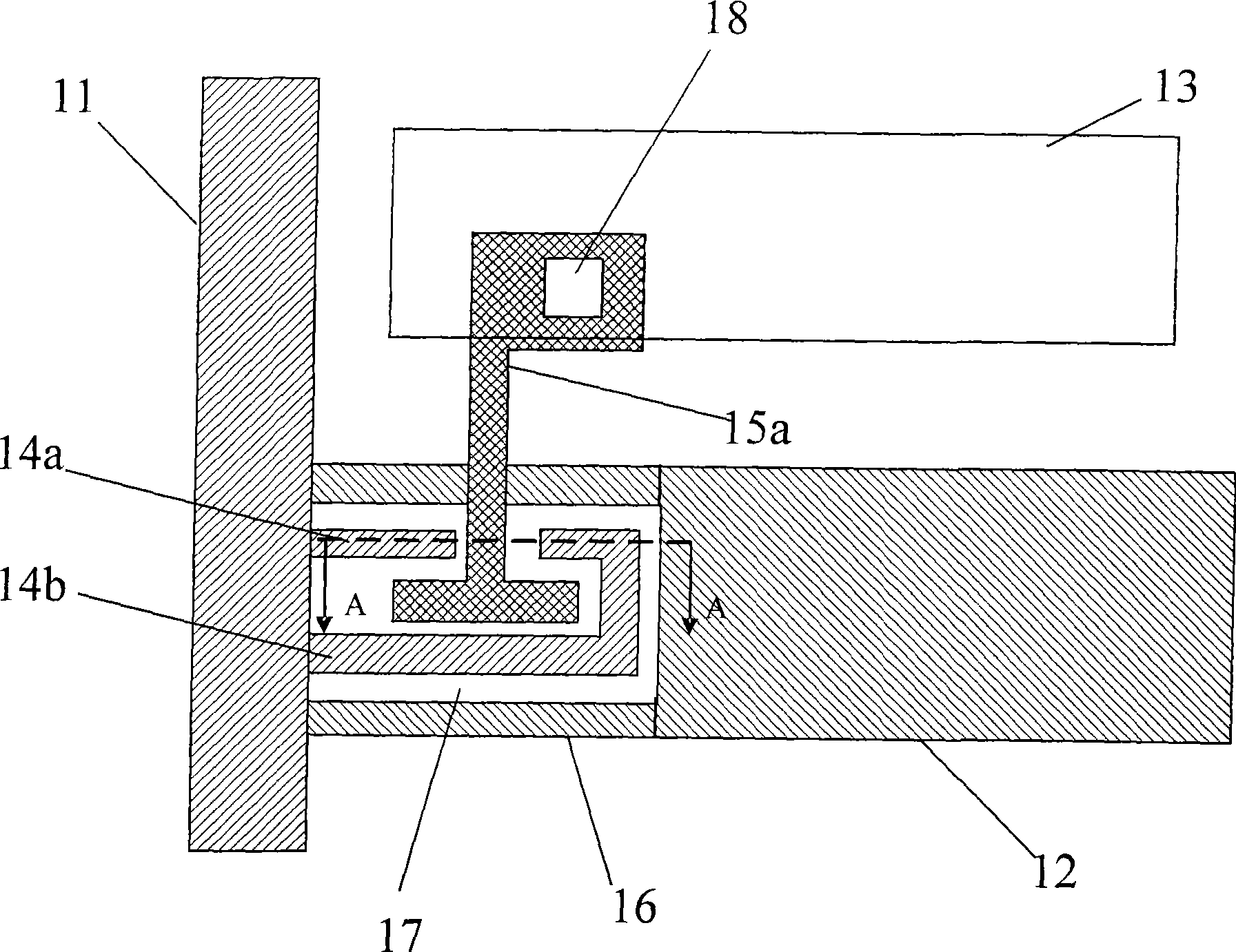
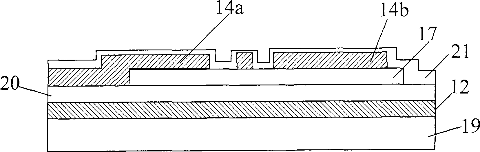
[0019] like figure 2 As shown, in the thin film transistor (Thin Film Transistor, hereinafter referred to as TFT) of the first embodiment of the present invention, the TFT includes a first drain electrode 14a, a second drain electrode 14b, a source electrode 15a and a gate electrode 16, and the drain electrode 14 It is connected to the data line 11, one end of the source electrode 15a is connected to the pixel electrode 13 through the contact hole 18, and the gate electrode 16 is connected to the scan line 12, forming a switch for controlling pixel voltage writing. The first drain electrode 14a and the second drain electrode 14b of the TFT are semi-closed lines and form a semi-closed area, and the other end of the source electrode 15a is a "T"-shaped line located between the first drain electrod...


PUM


Abstract

The invention relates to a thin-film transistor and a liquid crystal display device using the thin-film transistor. The thin film transistor comprises a first drain electrode, a second drain electrode, a source electrode and a grid electrode, wherein a semi-close area is formed by the first drain electrode and the second drain electrode, and one end of the source electrode is positioned in the semi-close area. The thin-film transistor can reduce the parasitic capacitance generated between the source electrode and the grid electrode and improve the display quality of images.

Description

technical field [0001] The invention relates to a thin film transistor and a liquid crystal display device, in particular to a thin film transistor and a liquid crystal display device with reduced parasitic capacitance. Background technique [0002] The liquid crystal display device is a passive display device. It cannot emit light by itself. It can only use ambient light or an external light source, but it only needs a small amount of energy to display patterns or characters, precisely because of its low power consumption and miniaturization. The characteristics make the liquid crystal display device a better display mode. The liquid crystal material used in the liquid crystal display device is an organic substance with both liquid and solid properties. Its rod-like structure is arranged in the liquid crystal cell, but its arrangement direction can be changed under the action of an electric field. [0003] Generally, a liquid crystal display device has an upper substrate a...

Claims


Application Information

Patent Timeline
Patent Type & Authority Applications(China)
IPC IPC(8): H01L29/786H01L29/417H01L27/12G02F1/1362
Inventor 李小和秦锋
Owner SHANGHAI SVA LIQUID CRYSTAL DISPLAY
Why Eureka
Try Eureka