Transparent conductive cathode contact structure for n type silicon

A transparent conductive electrode, transparent conductive technology, applied in the direction of circuits, electrical components, semiconductor devices, etc.

Inactive Publication Date: 2009-05-20
RONGGAO PV SOLAR DEV CO LTD
View PDF1 Cites 7 Cited by
  • Summary
  • Abstract
  • Description
  • Claims
  • Application Information

AI Technical Summary

Problems solved by technology

The lithium fluoride LiF layer inserted between the n-type silicon and the transparent conductive electrode can overcome the shortcomings of the existing transparent conductive electrode with

Method used


Image

  • Transparent conductive cathode contact structure for n type silicon
  • Transparent conductive cathode contact structure for n type silicon
  • Transparent conductive cathode contact structure for n type silicon

Examples


Embodiment 1

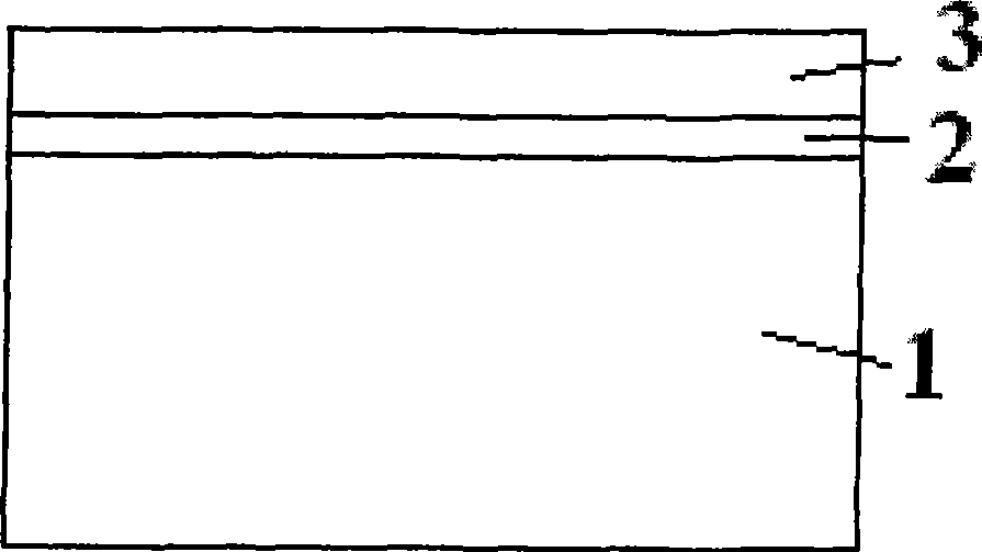
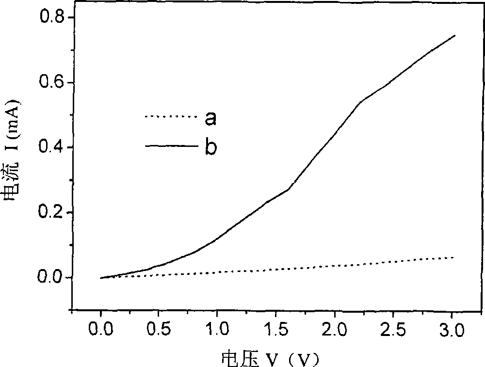
[0025] On the n-type single crystal silicon is a lithium fluoride LiF layer with a thickness of 0.5nm deposited by thermal evaporation, and then on the lithium fluoride LiF layer is an ITO transparent conductive electrode deposited by magnetron sputtering. The work function of the ITO transparent conductive electrode is greater than that of n-type single crystal silicon. figure 2 The I-V effect of this n-type monocrystalline silicon / LiF / ITO electrode is given in , curve a is the I-V curve of n-type monocrystalline silicon / ITO electrode without lithium fluoride LiF intercalation layer, and curve b is the n-type The I-V curve of the single crystal silicon / LiF / ITO electrode is compared. It can be seen that the insertion of the lithium fluoride LiF layer reduces the contact barrier of the n-type single crystal silicon / ITO electrode and improves the electron collection efficiency.

Embodiment 2

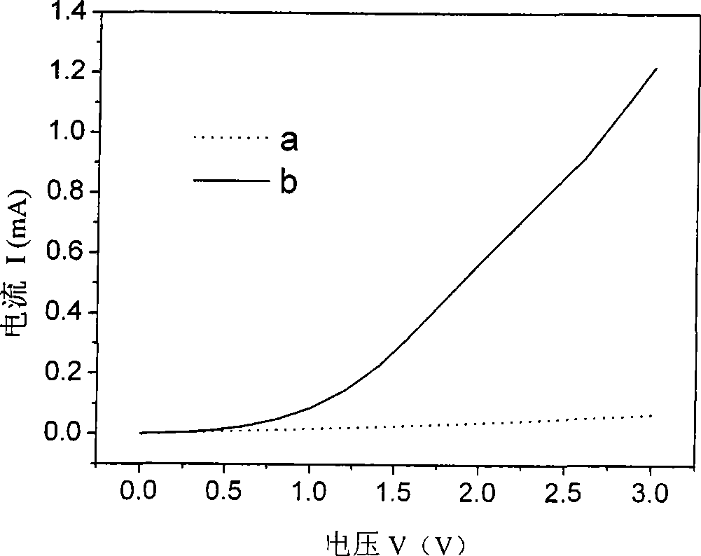
[0027] On the n-type polysilicon is a lithium fluoride LiF layer with a thickness of 1.5nm deposited by thermal evaporation, and then on the lithium fluoride LiF layer is an AZO transparent conductive electrode deposited by magnetron sputtering. The work function of the AZO transparent conductive electrode is greater than that of n-type polysilicon. image 3 The I-V effect of this n-type polysilicon / LiF / AZO electrode is given, the curve a is the I-V curve of the n-type polysilicon / AZO electrode without lithium fluoride LiF intercalation layer, and the curve b is this n-type polysilicon / LiF / AZO electrode It can be seen from the comparison that the insertion of lithium fluoride LiF layer reduces the contact barrier of n-type polysilicon / AZO electrode and improves the electron collection efficiency.

Embodiment 3

[0029] On the n-type amorphous silicon is a lithium fluoride LiF layer with a thickness of 2 nm deposited by thermal evaporation, and then on the lithium fluoride LiF layer is an ITO transparent conductive electrode deposited by magnetron sputtering. The work function of the ITO transparent conductive electrode is greater than that of n-type amorphous silicon. image 3 The I-V effect of this n-type amorphous silicon / LiF / ITO electrode is given in , the curve a is the I-V curve of the n-type amorphous silicon / ITO electrode without lithium fluoride LiF intercalation layer, and the curve b is the n-type amorphous silicon The comparison of the I-V curves of the crystalline silicon / LiF / ITO electrode shows that the insertion of the lithium fluoride LiF layer reduces the contact barrier of the n-type amorphous silicon / ITO electrode and improves the electron collection efficiency.


PUM

PropertyMeasurementUnit
Thicknessaaaaaaaaaa

Abstract

The invention relates to a transparent conductive cathode contact structure used on n-type silicon, which is basically characterized in that a LiF layer (2) is positioned on the n-type silicon (1), and then a transparent conductive electrode (3) is positioned on the Lif layer (2). The Lif layer (2) can reduce the contact potential barrier between the n-type silicon (1) and the transparent conductive electrode (3) to improve the collection or injection efficiency of electrons.

Description

technical field [0001] The invention relates to the field of semiconductors, in particular to a transparent conductive cathode contact structure for n-type silicon. Background technique [0002] A transparent conductive electrode is a very important optoelectronic material. A good transparent conductive electrode needs to meet the following requirements: it has a conductivity close to that of a metal to realize the electrode function; it has a high transmittance in the visible light or wider spectral range to facilitate the light Exit or enter; and have a suitable work function to reduce the carrier transport barrier and improve its injection or extraction efficiency. [0003] indium tin oxide In 2 o 3 :Sn(ITO), zinc aluminum oxide ZnO:Al(AZO) represented by inorganic oxide transparent conductive film (TCO) has been widely used in solar cells, displays, light-emitting diodes and other optoelectronic devices because of their excellent performance. However, TCOs have been b...

Claims


Application Information

Patent Timeline
IPC IPC(8): H01L33/00H01L31/0224H01L33/42
Inventor 赵雷王文静
Owner RONGGAO PV SOLAR DEV CO LTD
Why Eureka
Try Eureka