Infrared receiver and manufacturing method thereof

A technology of infrared detectors and manufacturing methods, applied in the direction of electric radiation detectors, manufacturing microstructure devices, semiconductor/solid-state device components, etc., can solve problems affecting product performance, reliability and yield, and achieve flattening problems, improve product yield and reliability, and prevent short circuits

Active Publication Date: 2009-06-03
ZHEJIANG DALI TECH +1
View PDF11 Cites 59 Cited by
  • Summary
  • Abstract
  • Description
  • Claims
  • Application Information

AI Technical Summary

Problems solved by technology

However, after the metal reflective layer pattern is formed, its surface is no longer flat, and the planarization problem will be accumulated in the subsequent process, thus

Method used


Image

  • Infrared receiver and manufacturing method thereof
  • Infrared receiver and manufacturing method thereof
  • Infrared receiver and manufacturing method thereof

Examples


Embodiment Construction

[0025] In order to better understand the technical content of the present invention, specific embodiments are given together with the attached drawings for description as follows.

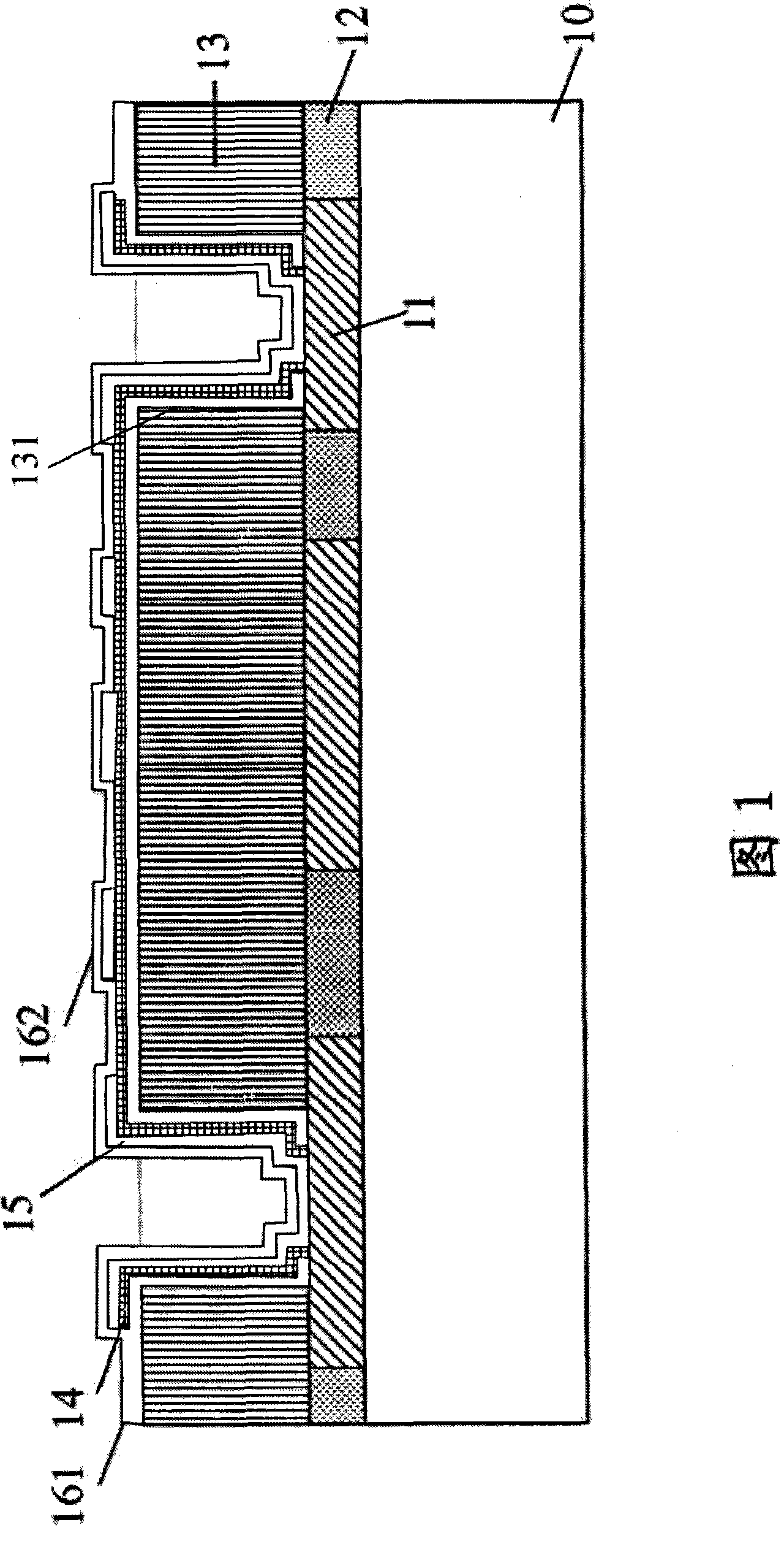
[0026] Please refer to FIG. 1 , which is a cross-sectional view of an infrared detector in a preferred embodiment of the present invention. This embodiment proposes an infrared detector, which can be used in places such as power network security detection, forest fire detection, and human body temperature detection.

[0027] The infrared detector includes a silicon substrate 10 , a metal reflective layer 11 , a dielectric layer 12 , a sacrificial layer 13 , a release protection layer 161 , a sensitive material detection layer 14 , a metal electrode 15 and a release protection layer 162 .

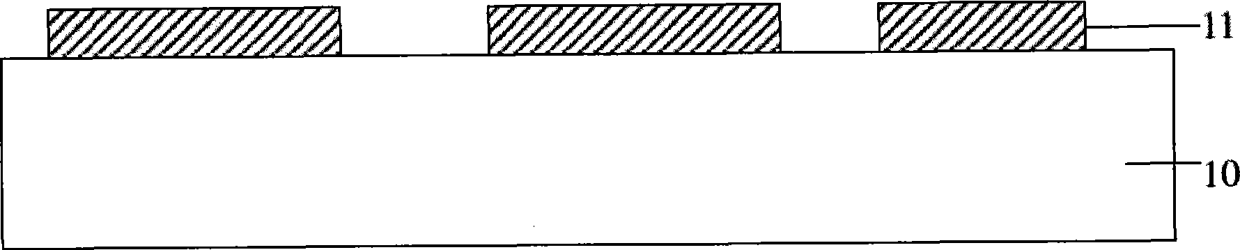
[0028] The metal reflective layer 11 is deposited on the silicon substrate 10, and grooves are carved by photolithography, etching and other processes to form a metal reflective pattern. Its function is to form a...


PUM


Abstract

The invention provides an infrared receiver and a manufacturing method thereof. A metallic reflecting layer, a dielectric layer, a sacrifice layer, a sensitive material detecting layer and a metallic electrode are precipitated on a silicon bulk of the infrared receiver in sequence. The metallic reflecting layer is provided with a metallic reflection pattern. The height of the dielectric layer and the height of the metallic reflecting layer are the same. The invention also provides the manufacturing method of the infrared receiver, comprising the following steps: the metallic reflecting layer is formed on the silicon bulk and patterning is carried out on the metallic reflecting layer; the dielectric layer is formed on the metallic reflecting layer and planarization is carried out on the dielectric layer; medium is etched and reserved on the surface of a metallic layer, and the height of the dielectric layer and the height of the metallic reflecting layer are confirmed to be the same; the sacrifice layer is precipitated; and a microbridge infrared absorption structure is fabricated.

Description

technical field [0001] The invention relates to a manufacturing process of an infrared detector, and in particular to an infrared detector and a manufacturing method thereof. Background technique [0002] Micro-electro-mechanical system (MEMS) technology has many advantages such as small, intelligent, executable, integrated, good process compatibility, and low cost, so it has begun to be widely used in many fields including the field of infrared detection technology. Infrared detector is a MEMS product that is widely used in the field of infrared detection technology. It uses a sensitive material detection layer (usually amorphous silicon or an oxide machine) to absorb infrared rays and convert them into electrical signals, thereby realizing thermal imaging. Features. [0003] Infrared detector technology is generally poorly compatible with CMOS technology, so it is difficult to achieve large-scale production in the early stage. In recent years, due to the gradual expansio...

Claims


Application Information

Patent Timeline
IPC IPC(8): B81B7/02G01J5/10B81C1/00
Inventor 康晓旭姜利军
Owner ZHEJIANG DALI TECH
Why Eureka
Try Eureka