Method for manufacturing semiconductor device

A manufacturing method and semiconductor technology, applied in semiconductor/solid-state device manufacturing, semiconductor devices, electric solid-state devices, etc., can solve problems such as increased cut-off current

Inactive Publication Date: 2009-06-03
SEMICON ENERGY LAB CO LTD
View PDF3 Cites 12 Cited by
  • Summary
  • Abstract
  • Description
  • Claims
  • Application Information

AI Technical Summary

Problems solved by technology

However, there is a tendency that the cut-off current also increases

Method used


Image

  • Method for manufacturing semiconductor device
  • Method for manufacturing semiconductor device
  • Method for manufacturing semiconductor device

Examples


Embodiment approach 1

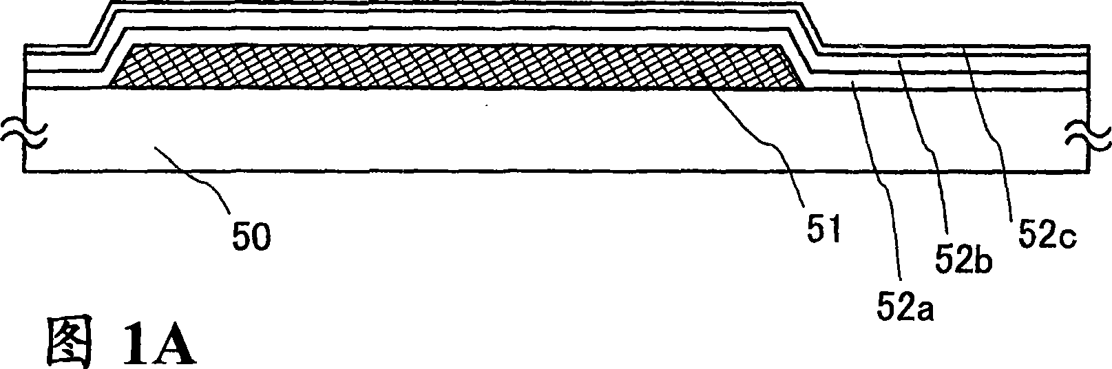
[0090] In this embodiment, referring to Fig. 1A to Figure 7B A manufacturing process of a thin film transistor used in a liquid crystal display device will be described. Figure 1A to Figure 3C is a sectional view showing a manufacturing process of a thin film transistor, and Figure 4 It is a top view of the connection area of ​​a thin film transistor and a pixel electrode in a pixel. In addition, FIG. 5 is a timing chart showing a method of forming a microcrystalline semiconductor film. Figure 6A with 6B An example of a reaction chamber for forming a microcrystalline semiconductor film is shown. Figure 7A with 7B show will Figure 6A with 6B The shown perspective view and plan view of an example of a plasma CVD (Chemical Vapor Deposition) apparatus in which reaction chambers are stacked in the vertical direction.

[0091] As for thin film transistors having microcrystalline semiconductor films, n-type thin film transistors have higher mobility than p-type thin fil...

Embodiment approach 2

[0153] This embodiment mode shows an example of a multi-chamber plasma CVD apparatus suitable for forming the microcrystalline semiconductor film constituting the TFT described in the first embodiment mode.

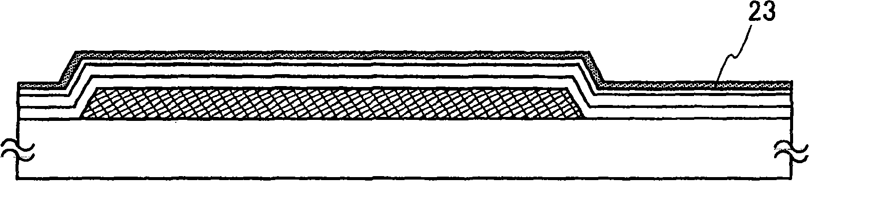
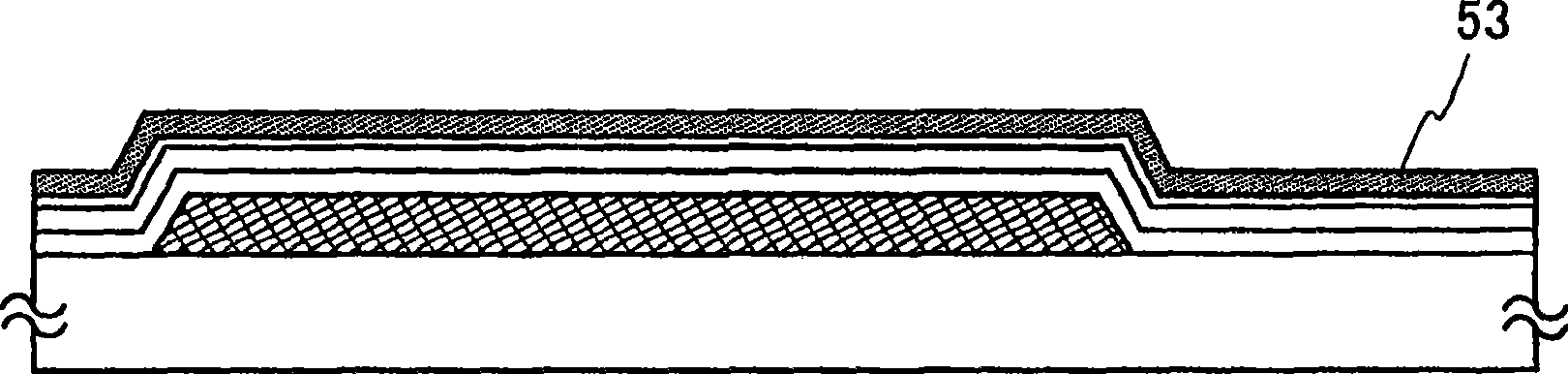
[0154] Figure 6A An example of the plasma CVD apparatus shown in Embodiment 1 is shown, in which a film formation chamber 204a, which is a processing chamber capable of maintaining a reduced-pressure atmosphere, is provided outside the reaction chamber 208a where the microcrystalline semiconductor film 53 is formed.

[0155] exist Figure 6A In this example shown, the reaction chamber 208a is grounded, the reference numeral 205a denotes a high-frequency power supply, and the reference numeral 221 denotes a first electrode (upper electrode, shower electrode, high-frequency electrode) having a hollow structure through which raw material gas can pass. , reference numeral 225 represents a grounded second electrode (lower electrode, ground electrode), reference numeral 206a ...

Embodiment approach 3

[0170] In this embodiment mode, a method of manufacturing a thin film transistor having excellent characteristics by selecting a gas used for forming a microcrystalline semiconductor film by a CVD method and a film forming method will be described.

[0171]In one method, the field-effect mobility of the TFT is improved by making the microcrystalline semiconductor film 23 obtained under the first film-forming condition in Embodiment 1 into an n-type. Specifically, when forming the microcrystalline semiconductor film under the first film-forming conditions, an n-type impurity element is added. As the n-type impurity element used at this time, phosphorus, arsenic, and antimony can be used. In particular, it is preferable to use inexpensive phosphorus as the phosphine gas.

[0172] Furthermore, by exposing the surface of the gate insulating film to phosphine gas, phosphorus is attached (or reacted) before nitrogen and oxygen are attached to the surface of the gate insulating film...


PUM


Abstract

In order to improve the quality of a microcrystalline semiconductor film which is formed at an early stage of deposition, a microcrystalline semiconductor film near an interface with a base insulating film is formed under a deposition condition in which a deposition rate is low but the quality of a film to be formed is high; then, a microcrystalline semiconductor film is further deposited at a deposition rate which is increased stepwise or gradually. The microcrystalline semiconductor film is formed in a reaction chamber which is provided in a deposition chamber with space around the reaction chamber, by a chemical vapor deposition method. Further, a scaling gas is supplied into the space to help place the reaction chamber in an ultrahigh vacuum, whereby the concentration of an impurity in the microcrystalline semiconductor film near the interface with the base insulating film is reduced.

Description

technical field [0001] The present invention relates to a semiconductor device having a circuit composed of thin film transistors (hereinafter also referred to as TFTs) and a method of manufacturing the same. For example, the present invention relates to electronic equipment incorporating, as a component, an electro-optical device typified by a liquid crystal display panel or a light-emitting display device having an organic light-emitting element. [0002] In this specification, a semiconductor device refers to all devices that can operate by utilizing semiconductor characteristics, and thus display devices such as electro-optical devices and light-emitting display devices, semiconductor circuits, and electronic equipment are all semiconductor devices. Background technique [0003] In recent years, a technique of constituting a thin film transistor (TFT) by using a semiconductor thin film (about several nm to several hundred nm in thickness) formed on a substrate having an ...

Claims


Application Information

Patent Timeline
Patent Type & Authority Applications(China)
IPC IPC(8): H01L21/00H01L21/336H01L21/205
CPCH01L29/78696H01L21/67184H01L27/1214H01L27/1288H01L29/04H01L21/0262H01L29/4908H01L29/458H01L21/67161H01L21/02381H01L21/205H01L21/786
Inventor 山崎舜平
Owner SEMICON ENERGY LAB CO LTD
Why Eureka
Try Eureka