Integrated circuit layout structure and manufacturing method thereof

A technology of integrated circuit and layout structure, applied in the direction of circuits, electrical components, electrical solid devices, etc., can solve problems such as copper metal residues, achieve the effects of improving yield, avoiding hot spots, and increasing line spacing

Inactive Publication Date: 2009-06-03
SEMICON MFG INT (SHANGHAI) CORP +1
View PDF0 Cites 1 Cited by
  • Summary
  • Abstract
  • Description
  • Claims
  • Application Information

AI Technical Summary

Problems solved by technology

[0005] In order to solve the problem of copper metal residue in the thin line area of ​​the integrated circuit layout after chemical mechanical polishing in the prior art, the purpose of the present invention is to provide an integrated circuit layout structure

Method used


Image

  • Integrated circuit layout structure and manufacturing method thereof
  • Integrated circuit layout structure and manufacturing method thereof
  • Integrated circuit layout structure and manufacturing method thereof

Examples


Embodiment Construction

[0016] The technical solution of the present invention will be described in detail below in conjunction with the accompanying drawings and specific embodiments.

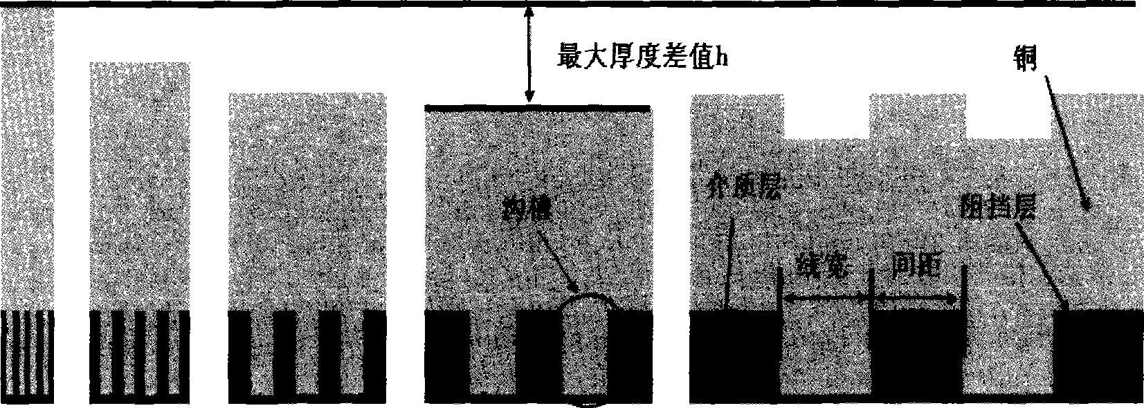
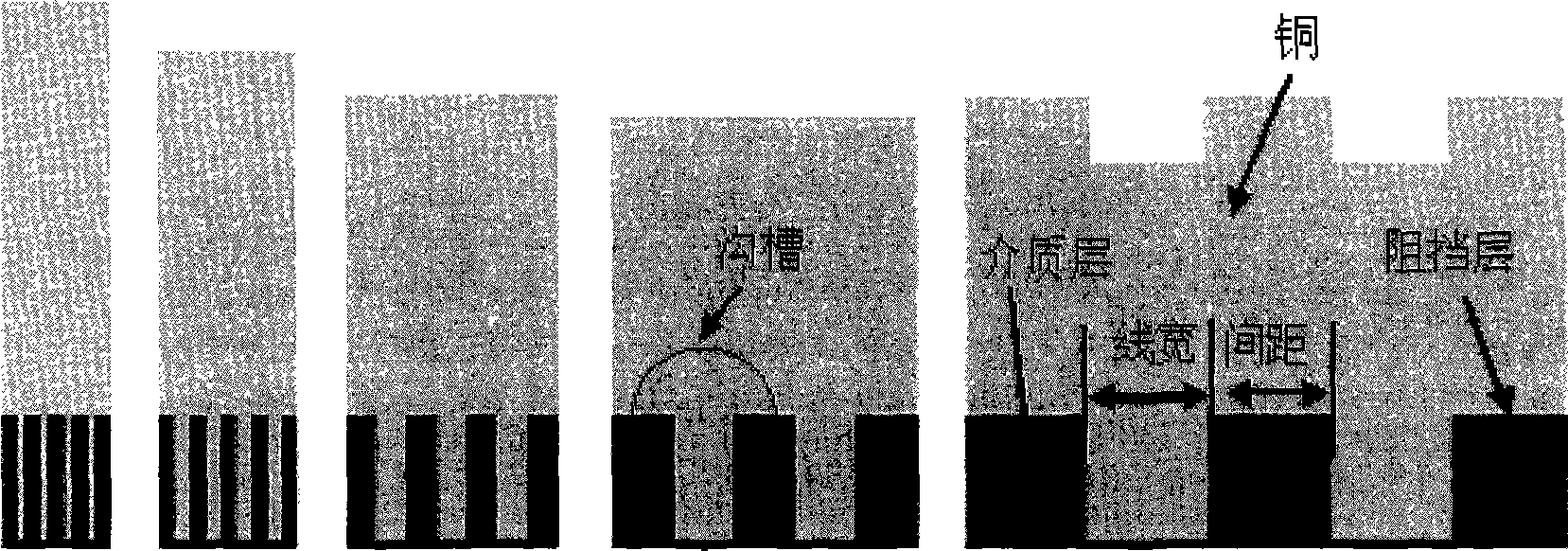
[0017] see image 3 , the present invention is a layout structure of an integrated circuit, the width of the copper wire in the thin line area is less than 0.2 microns, the line spacing in the thin line area is twice the width of the copper wire, and the area of ​​the copper wire is 30% of the total area of ​​the layout, This structure reduces the copper growth thickness in the thin line area, and the copper growth of different structures is relatively uniform, which reduces the surface fluctuation before the CMP process, reduces the burden of the CMP process, improves the chemical mechanical polishing ability, and will obtain the optimal planarization effect.

[0018] A manufacturing method of an integrated circuit layout, under the condition that the total area of ​​the layout is allowed, during the layout and wiri...


PUM


Abstract

The invention relates to an integrated circuit layout structure and a manufacturing method thereof belonging to the technical field of the manufacturing process of an integrated circuit and the layout design. In order to solve the problem in the prior art that after chemical mechanical polishing, copper metal in a thin line area of the integrated circuit layout is left, the invention provides the integrated circuit layout structure and the manufacturing method thereof. By increasing the line space in the thin line area, the growth thickness of the copper in the thin line area is lowered, and copper with different structures grows evenly, thus reducing the load of chemical mechanical polishing, improving planarization capacity, avoiding heat spots in the thin line area and improving yield of products.

Description

technical field [0001] The invention relates to the technical field of integrated circuit manufacturing technology and layout design, in particular to an integrated circuit layout structure and a manufacturing method thereof. Background technique [0002] Chemical Mechanical Polishing (CMP) is a surface planarization process used in the manufacture of integrated circuits. It is a combined technology of chemical corrosion and mechanical polishing. Forming a smooth and flat surface on the surface of the medium is recognized as the best material global planarization method in the VLSI stage. This method can not only obtain a more perfect surface, but also obtain a higher polishing rate. Integrated Circuit (IC) manufacturing technology develops at a speed of doubling the integration level every 18 months according to Moore's Law, but when the feature size of integrated circuits drops below 90 nanometers, IC manufacturing technology encounters unprecedented challenges. Chemical ...

Claims


Application Information

Patent Timeline
Patent Type & Authority Applications(China)
IPC IPC(8): H01L23/522G06F17/50
Inventor 阮文彪陈岚李志刚
Owner SEMICON MFG INT (SHANGHAI) CORP
Why Eureka
Try Eureka