Method for producing heat insulation antiblocking cavity based on silicon substrate

A silicon substrate, anti-adhesion technology, applied in the process of producing decorative surface effects, manufacturing microstructure devices, coatings, etc., can solve the long time of etching and releasing the sacrificial layer, the process is cumbersome, and it is not suitable for large Large-scale production and other issues to achieve the effect of strong practical value, simple process steps, and high production efficiency

Inactive Publication Date: 2009-06-10
INST OF MICROELECTRONICS CHINESE ACAD OF SCI
View PDF0 Cites 1 Cited by
  • Summary
  • Abstract
  • Description
  • Claims
  • Application Information

AI Technical Summary

Problems solved by technology

[0005] As we all know, this method is cumbersome and takes a long time to etch and release the sacrificial layer, which is not suitable for mass production.

Method used


Image

  • Method for producing heat insulation antiblocking cavity based on silicon substrate
  • Method for producing heat insulation antiblocking cavity based on silicon substrate
  • Method for producing heat insulation antiblocking cavity based on silicon substrate

Examples


Embodiment Construction

[0028] In order to make the object, technical solution and advantages of the present invention clearer, the present invention will be described in further detail below in conjunction with specific embodiments and with reference to the accompanying drawings.

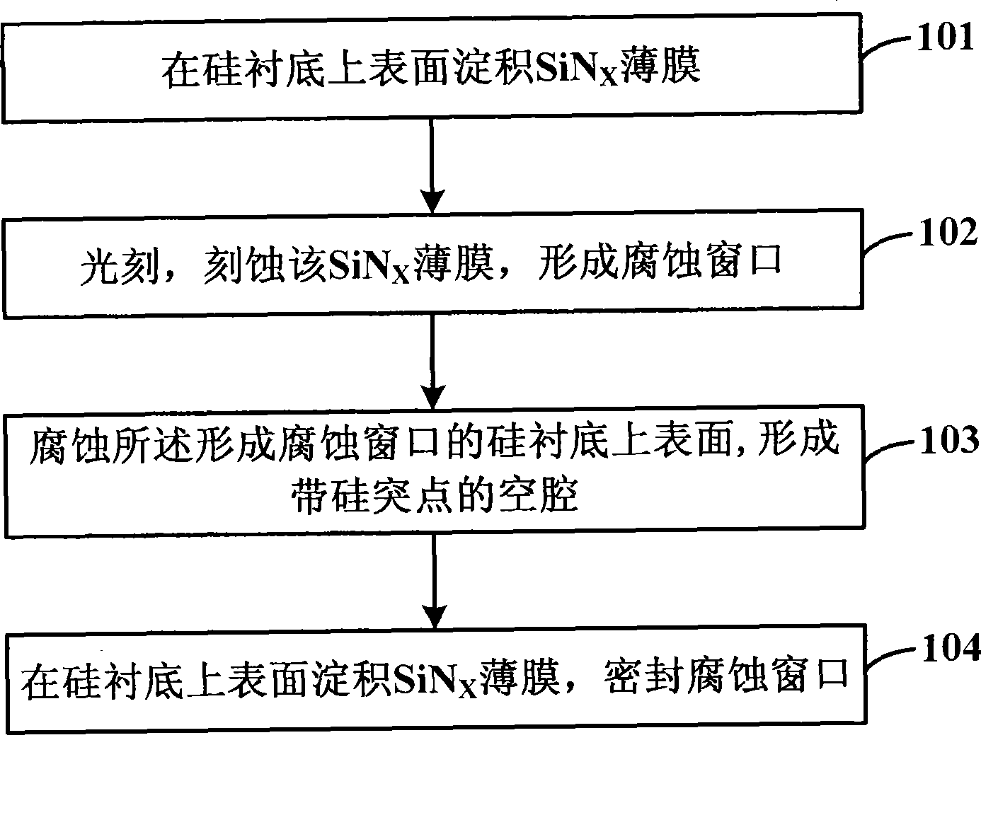
[0029] Such as figure 1 as shown, figure 1 It is a flowchart of a method for manufacturing a heat-insulating anti-adhesion cavity based on a silicon substrate provided by the present invention, and the method includes the following steps:

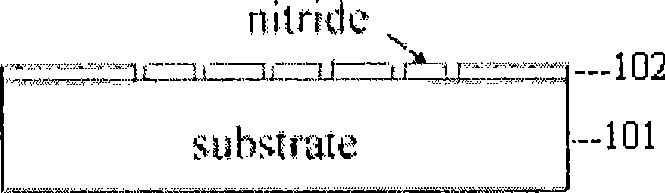
[0030] Step 101: Depositing SiN on the surface of the silicon substrate X film;

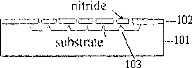
[0031] Step 102: photolithography, etch the SiN X thin film, forming a corrosion window;

[0032] Step 103: Etching the upper surface of the silicon substrate forming the etching window to form a cavity with silicon bumps;

[0033] Step 104: Deposit SiN on the surface of the silicon substrate X Thin film, seals corrosion windows.

[0034] The above step 101 includes: depositing SiN on the silicon ...


PUM

PropertyMeasurementUnit
thicknessaaaaaaaaaa
thicknessaaaaaaaaaa

Abstract

The invention discloses an adiabatic anti-adhesion cavity manufacturing method based on silicon substrates. The method comprises the steps of depositing a SiNX film on the upper surface of a silicon substrate, photoetching and etching the SiNX film so as to form a corrosion window, corroding the upper surface of the silicon substrate where the corrosion window is formed, forming a cavity with silicon protruding points, depositing the SiNX film on the upper surface of the silicon substrate and sealing the corrosion window. The method provided by the invention has the advantages of simple process steps, low cost, high production efficiency, stable process, high practical value and capability of adapting to the requirements of mass production.

Description

technical field [0001] The invention relates to the technical field of MEMS manufacturing in microelectronic technology, in particular to a method for manufacturing a heat-insulating and anti-adhesion cavity based on a silicon substrate. Background technique [0002] Among MEMS devices, quite a few are devices containing adiabatic cavities. For example, a thermistor is made on a thin film on an adiabatic cavity to measure some physical quantities based on thermal effects (such as speed, shear force, etc.). [0003] The formation of the thermally insulating cavity can be done by bulk silicon machining bonding process, or by micromachining the silicon substrate surface. Silicon-based surface micromachining technology is an important technology, which avoids vertical bulk silicon deep processing, has better compatibility with integrated circuit technology, and is conducive to the integration of devices and processing circuits. [0004] In the micromachining process of the sil...

Claims


Application Information

Patent Timeline
Patent Type & Authority Applications(China)
IPC IPC(8): B81C1/00
Inventor 石莎莉陈大鹏欧毅景玉鹏叶甜春
Owner INST OF MICROELECTRONICS CHINESE ACAD OF SCI
Why Eureka
Try Eureka