Encapsulation structure and method for applying guidance type light emitting diode device
A light-emitting diode and application-oriented technology, which is applied in the field of packaging structure of application-oriented light-emitting diode devices to achieve the effects of improving light extraction efficiency and spot quality, improving efficiency and reducing volume
- Summary
- Abstract
- Description
- Claims
- Application Information
AI Technical Summary
Problems solved by technology
Method used
Image
Examples
Embodiment 1
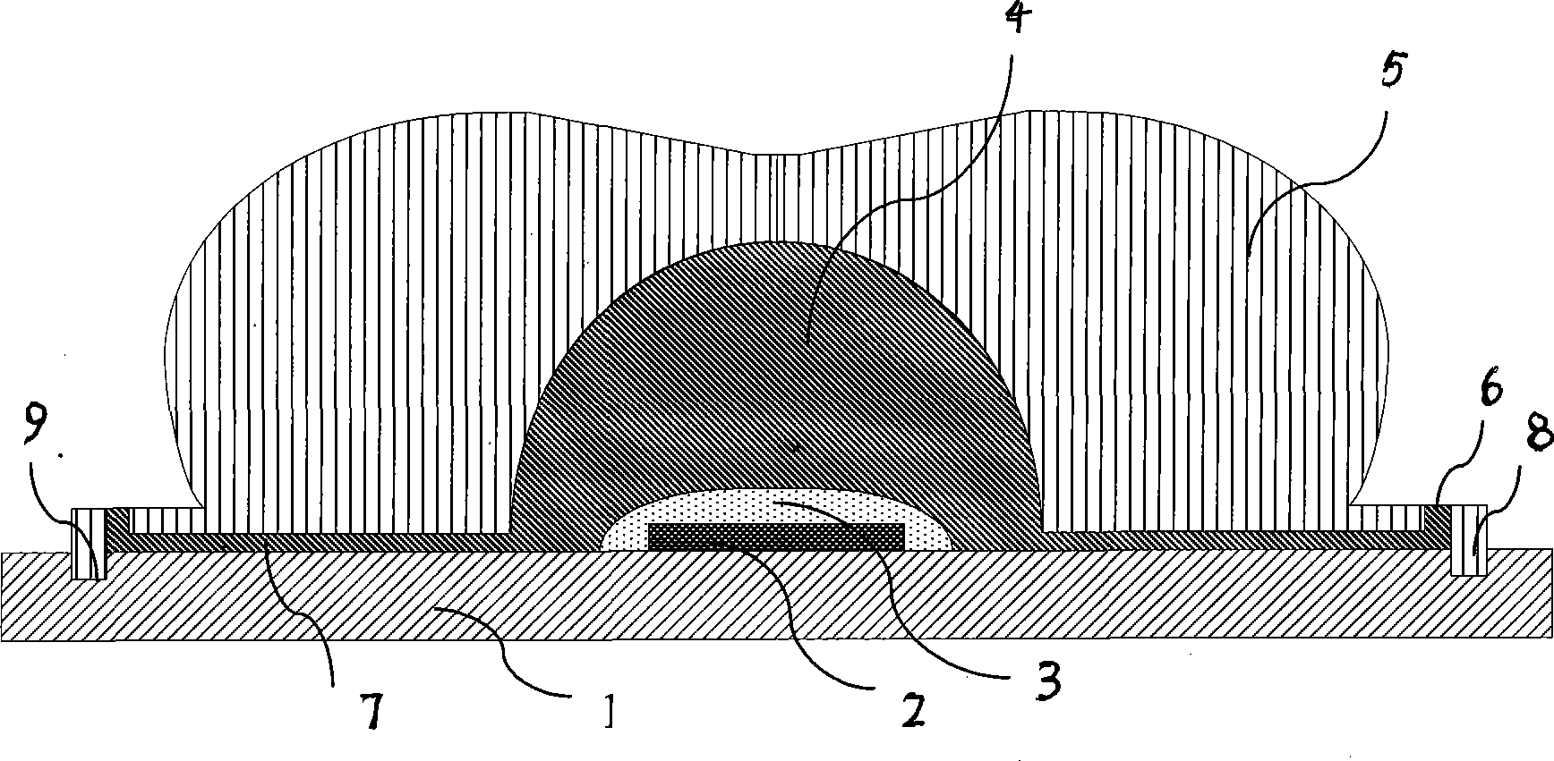
[0042] like Figure 4 Shown is the encapsulation flow chart of the encapsulation method 1 of the present invention. First, fix the light emitting diode chip 2 on the packaging package 1 through silver paste or solder or other bonding materials, and complete the electrical connection between the light emitting diode chip 2 and the package package 1 by punching gold wires or other electrode interconnection methods. interconnection. Phosphor powder glue 3 is wrapped LED chip 2 and cured ( Figure 4 a). Then, the free-form surface lens 5 obtained by mold manufacturing or precision machining is fixed on the package package 1 through the fixing structure 8 on the free-form surface lens and the fixing groove 9 on the package package. The fixation structures 8 and 9 are in natural contact or Adhesive bonding ( Figure 4 b). Then through the glue injector 11, the encapsulating colloid 4 is poured into the glue injection hole 6 of the free-form surface lens, and the encapsulating c...
Embodiment 2
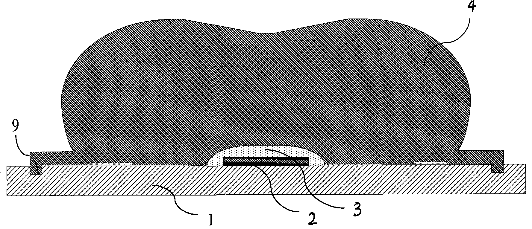
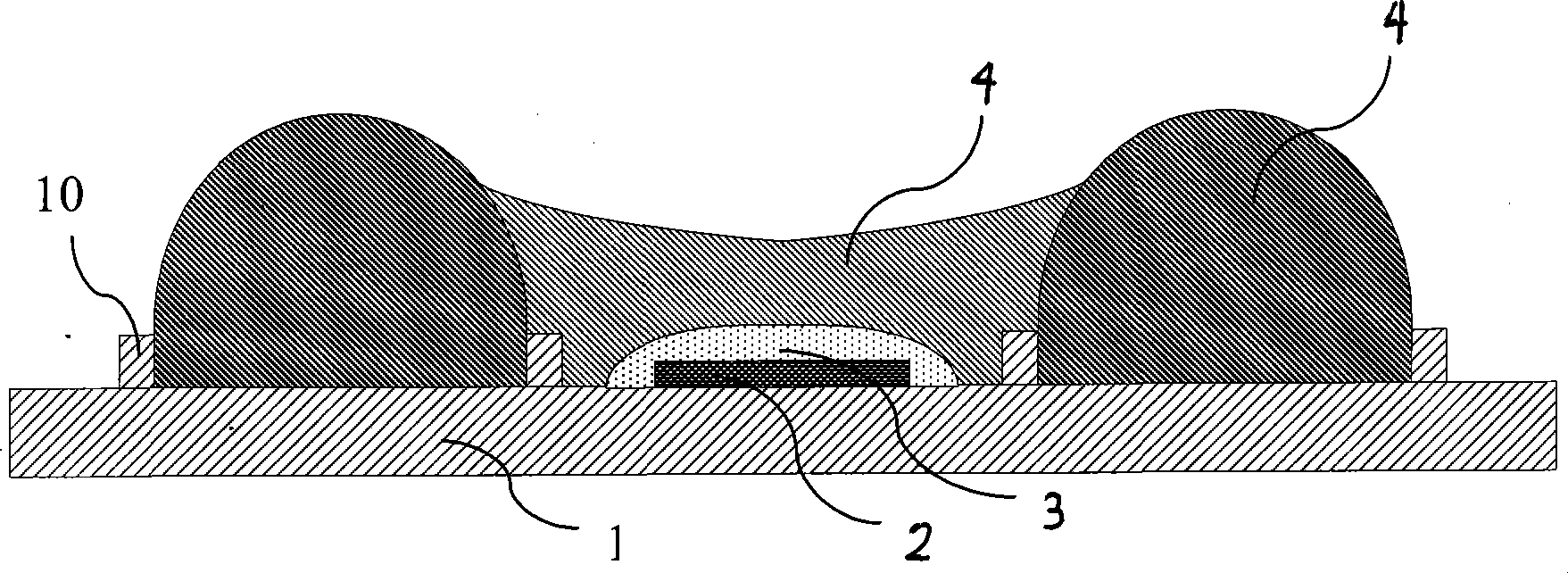
[0044] like Figure 5Shown is the encapsulation flow chart of the encapsulation method 2 of the present invention. First, obtain the light-emitting diode chip 2 ( Figure 5 a). Then, inject the encapsulant 4 into the encapsulation shell 1 through the glue injector 11, so that the encapsulant 4 can be self-flowing on the encapsulation shell without restraint, or constrained by the convex structure 10 that restricts the flow of the encapsulant on the encapsulation shell. bottom self-flow forming, and wrapping the light-emitting diode chip 2 ( Figure 5 b). Then, the free-form surface lens 5 is obtained by mold manufacturing or precision machining, and the encapsulation colloid 4 is squeezed from top to bottom, so that the encapsulation colloid 4 is completely surrounded by the upper surface of the packaging tube, the upper surface of the chip, the base surface of the lens, and the light incident surface. cavity, excess encapsulation colloid and air are discharged from the in...
Embodiment 3
[0046] like Image 6 Shown is the encapsulation flow chart of the encapsulation method 3 of the present invention. First, obtain the light-emitting diode chip 2 ( Image 6 a). Then, the free-form surface lens mold 12 is aligned and fixed on the package shell 1 ( Image 6 b). Then from the free-form surface lens mold injection hole 13, the encapsulation compound 4 is poured into the cavity surrounded by the package shell upper surface, the chip upper surface and the inner surface of the mold, and the encapsulation compound 4 is filled with the entire cavity ( Image 6 c). Finally, curing the encapsulation colloid 4, demolding, and completing the encapsulation of the light-emitting diode free-form surface lens ( Image 6 d).
PUM
 Abstract
Description
Claims
Application Information


