Organic electroluminescent devices of laminated construction
An electroluminescent device, organic technology, applied in the direction of electro-solid devices, electrical components, organic chemistry, etc., can solve the problems of high evaporation temperature, low electron mobility of organic materials, difficult process implementation, etc., and achieves simple preparation process, Effects of low film formation temperature and improved device power efficiency
- Summary
- Abstract
- Description
- Claims
- Application Information
AI Technical Summary
Problems solved by technology
Method used
Image

Examples
Embodiment 1
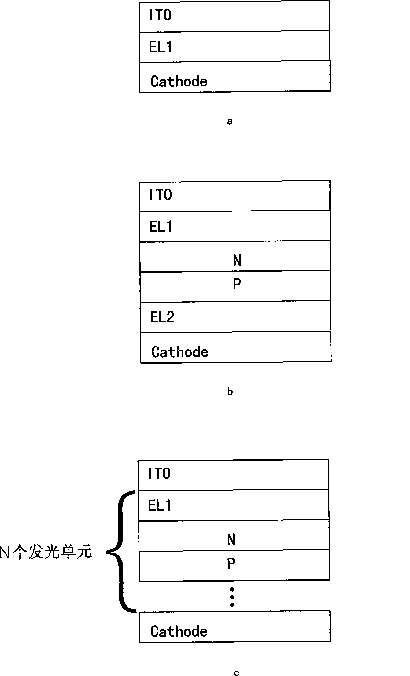
[0041] Device structure:
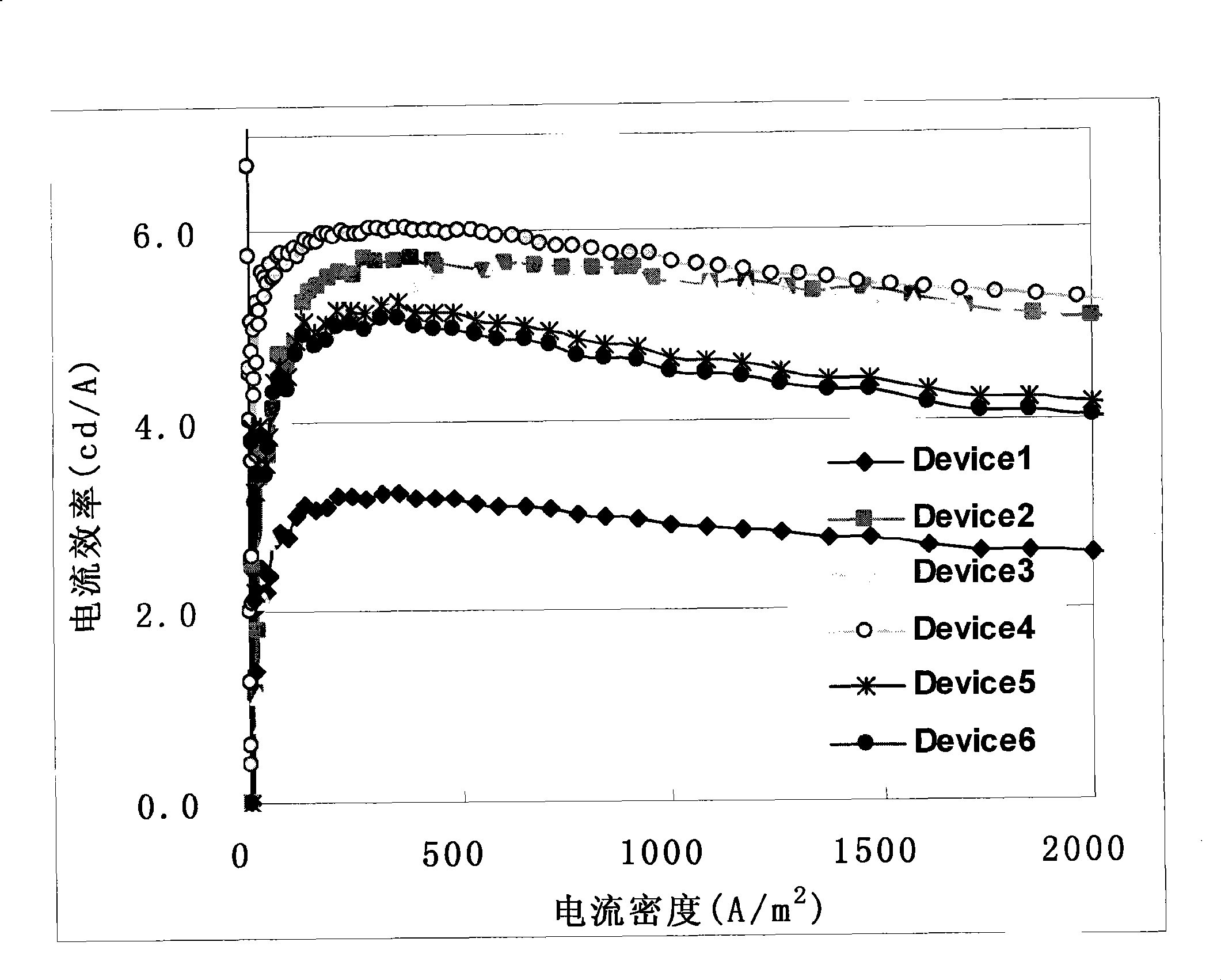
[0042] Device1: ITO / HIL / EL1 / Li 3 N / Al
[0043] Device2-6: ITO / HIL / EL1 / N / P / EL2 / Li 3 N / Al
[0044] Where EL1 in Device 2-6 is: NPB(40nm) / Alq3(30nm) / (compound C1, C11, C21, C31 or Alq 3 )(20nm)
[0045] N / P in Device 2-6 is: (compound C1, C11, C21, C31 or Alq 3 ) doped with 10% Li3N / V 2 o 5
[0046] Device: EL2 in 2-6 is: NPB(40nm) / Alq 3 (30nm) / (compound C1, C11, C21, C31 or Alq3 )
[0047] With the ITO conductive glass substrate etched with specific patterns as the substrate, the substrate is ultrasonically cleaned in deionized water containing cleaning solution. The temperature of the cleaning solution is about 60°C, and then the cleaned substrate is cleaned Dry it, put it into the evaporation chamber to evaporate the hole injection layer, EL1, the compound Li3N / P connection layer, E12, and the electrode in sequence, and the pressure of the chamber during the evaporation process is lower than 5.0×10 -3 Pa. In this embodiment, the N-type co...
Embodiment 2
[0050] Device structure:
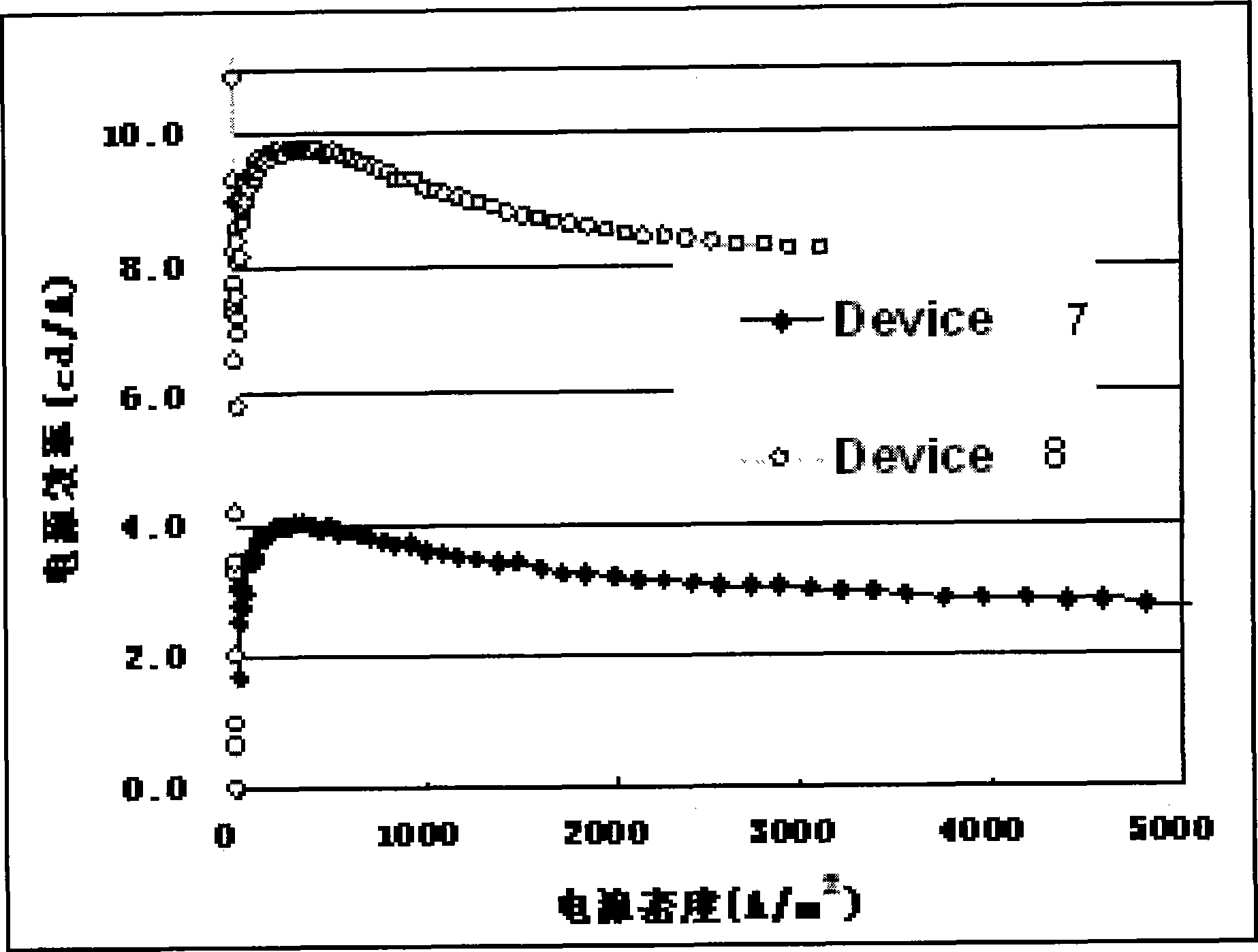
[0051] Device 7: ITO / HIL / EL3 / Li 3 N / Al
[0052] Device 8: ITO / HIL / EL3 / N / P / EL4 / Li 3 N / Al
[0053] Where EL3 is: NPB(40nm) / GH:GD / compound C1(20nm)
[0054] N / P is: Compound C1: 10% Li3N / HAT
[0055] EL4 is: NPB(40nm) / GH:GD / compound C1(20nm)
[0056] With the ITO conductive glass substrate etched with specific patterns as the substrate, the substrate is ultrasonically cleaned in deionized water containing cleaning solution. The temperature of the cleaning solution is about 60°C, and then the cleaned substrate is cleaned Dry it, put it into the evaporation chamber to evaporate the hole injection layer, EL1, N / P connection layer, E12, and electrode in sequence, and the pressure of the chamber during the evaporation process is lower than 5.0×10 -3 Pa. In this embodiment, the N-type connection layer is prepared by dual-source doping and co-evaporation of compound C1 and lithium nitride.
[0057] from figure 2 It can be seen that the current effici...
Embodiment 3
[0062] Device 9: ITO / HAT / EL5 / Alq 3 :Li / Al
[0063] Device 10: ITO / m-MTDATA:F1TCNQ / EL5 / Alq 3 : Doped with 10% Li / m-MTDATA: F1TCNQ / EL5 / Alq 3 : Li / Al, where N / P is Alq 3 : doped with 10% Li / m-MTDATA:F1TCNQ.
[0064] Device 11: ITO / MoO 3 / EL5 / compound C1: doped with 10% Li 3 N / MoO 3 / EL5 / Compound C1:Li 3 N / Al, where N / P is compound C1: doped with 10% Li 3 N / MoO 3 .
[0065] Device 12: ITO / m-MTDATA:F1TCNQ / EL5 / Compound C1: Doped with 10% Li 3 N / m-MTDATA: F1TCNQ / EL5 / Compound C1: doped with 10% Li 3 N / Al, where N / P is compound C1: doped with 10% Li 3 N / m-MTDATA:F1TCNQ.
[0066] Device 13: ITO / HAT / EL5 / Compound C1: doped with 10% Li 3 N / HAT / EL5 / compound C1: doped with 10% Li 3 N / Al, where N / P is compound C1: doped with 10% Li 3 N / HAT.
[0067] Device 14: ITO / HAT / EL5 / compound C1: doped with 70% Li 3 N / HAT / EL5 / compound C1: doped with 70% Li 3 N / Al, where N / P is compound C1: doped with 70% Li 3 N / HAT.
[0068] EL5 is: NPB / Alq 3 :C545T / Alq 3
[0069] Table 2 is a com...
PUM
 Abstract
Description
Claims
Application Information
 - R&D
- Intellectual Property
- Life Sciences
- Materials
- Tech Scout
- Unparalleled Data Quality
- Higher Quality Content
- 60% Fewer Hallucinations
Browse by: Latest US Patents, China's latest patents, Technical Efficacy Thesaurus, Application Domain, Technology Topic, Popular Technical Reports.
© 2025 PatSnap. All rights reserved.Legal|Privacy policy|Modern Slavery Act Transparency Statement|Sitemap|About US| Contact US: help@patsnap.com