

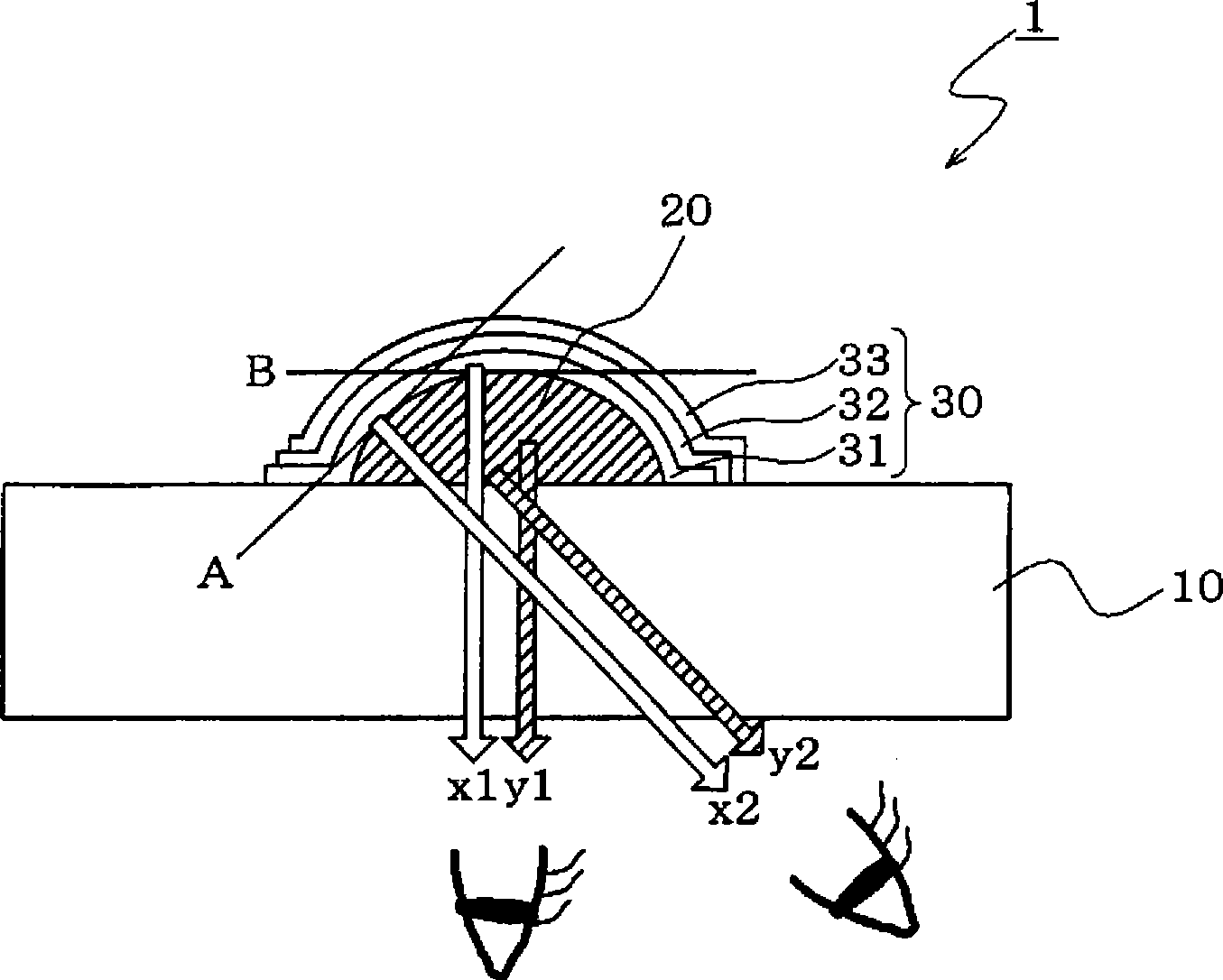
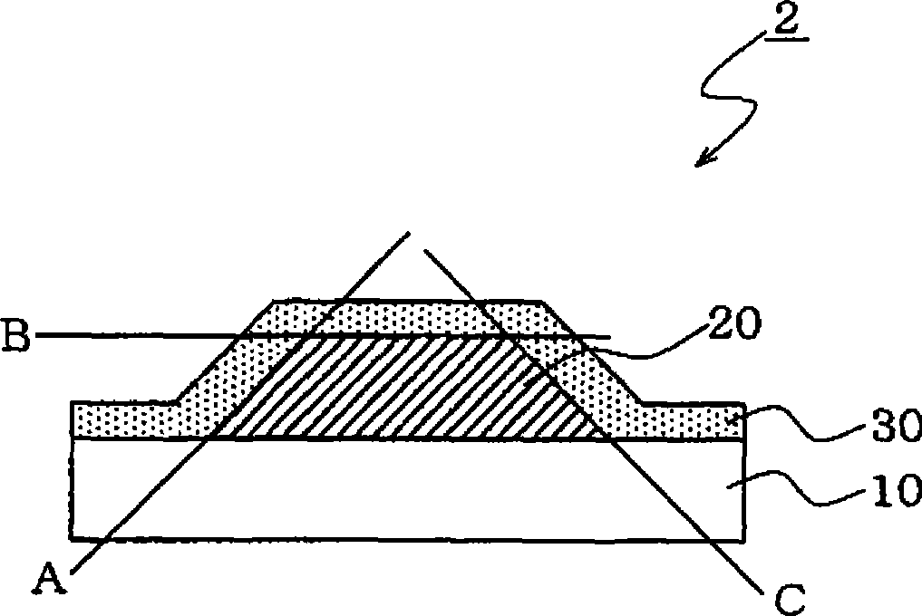
Light emitting device
A light-emitting device and light-emitting surface technology, which is applied in the fields of organic electroluminescent light-emitting devices and white light-emitting devices, can solve problems such as limited use of surfaces, and achieve the effects of improving luminous brightness, reducing adverse effects, and improving viewing angle dependence
- Summary
- Abstract
- Description
- Claims
- Application Information
AI Technical Summary
Problems solved by technology
Method used
Image

Examples
manufacture example 1
[0304] Modulation of Semiconductor Nanocrystalline Fluorescent Dielectric Material 1
[0305] 0.5 g of cadmium acetate dihydrate and 1.6 g of tetradecylphosphonic acid (TDPA) were added to 5 ml of trioctylphosphine (TOP). The solution was heated to 230°C under nitrogen atmosphere and stirred for 1 hour. After cooling to 60° C., 2 ml of a TOP solution containing 0.2 g of selenium was added as a raw material solution.
[0306] 10 g of trioctylphosphine oxide (TOPO) was placed in a three-necked flask, and vacuum-dried at 195° C. for 1 hour. Use nitrogen to return to atmospheric pressure, directly heat to 270° C. under nitrogen atmosphere, and add 1.5 ml of the above raw material solution while stirring the system. The reaction (nuclear growth reaction) proceeds while constantly checking the fluorescence spectrum of the reaction solution. When the nanocrystal has a fluorescence peak at 615 nm, the reaction solution is cooled to 60° C. to stop the reaction.
[0307] 20 ml of bu...
manufacture example 2
[0312] Modulation of Semiconductor Nanocrystalline Fluorescent Dielectric Material 2
[0313] To synthesize indium phosphide (InP) semiconductor nanocrystals, fresh In(OH) 3 0.02g (0.1mmol) was dissolved in HPA0.5g (3mmol) and TOPO3.5g. Next, the solution was cooled to 120-130° C., and argon gas was flowed into the reaction system. After depressurizing for 20-30 minutes, argon gas was further flowed in for 10-15 minutes. In order to remove all the water and oxygen absorbed by the reaction system, this process of argon gas flow and depressurization was repeated 3 times. After heating the reaction mixture to 300°C, inject the solution containing P(TMS) 3 2 g of a stock solution of 0.0277 g (0.1 mmol), TOP 1.8 g and toluene 0.2 g. To grow the nanocrystals, the reaction mixture was cooled to 250°C. After the nanocrystal reaches the desired particle size, the sheathed resistance heater is quickly taken out, and the reaction solvent is cooled to stop the reaction. After the tem...
manufacture example 3
[0316] Preparation of fluorescent medium material 3 using organic phosphor (perylene dye)
[0317] As a perylene-based dye, 0.3 wt% (relative solid content) of the compound represented by the following formula (Ia), 0.6 wt% (relative solid content) of the compound represented by the following formula (IIa) and 0.6 wt% (relative solid content) of the compound represented by the following formula (IIIa) 0.6 wt% of the compound (relative to solid content) was dissolved in the base resin in the same manner as in Production Example 1 to prepare a fluorescent medium material 3 using a perylene-based dye.
[0318] [chemical 9]
[0319]
PUM
| Property | Measurement | Unit |
|---|---|---|
| Film thickness | aaaaa | aaaaa |
Abstract
Description
Claims
Application Information