Printing device and printing method for integrating electronic components

A technology for electronic components and printing devices, applied in electrical components, printing devices, printing and other directions, can solve the problems of unfavorable wiring modification, waste of resources, complicated processing technology, etc., and achieve the effect of good processing flexibility, easy operation and simple process

Active Publication Date: 2009-06-24
CARERAY DIGITAL MEDICAL TECH CO LTD
View PDF0 Cites 53 Cited by
  • Summary
  • Abstract
  • Description
  • Claims
  • Application Information

AI Technical Summary

Problems solved by technology

[0004] The above-mentioned wiring method has the following disadvantages: the fixed investment in process equipment is high, the processing technology is complicated, the area of ​​the processed electronic device is too large, which is not conducive to the integration of the device, and the processing of the PCB board needs to corrode the copper clad laminate, which not only wastes resources but also pollutes the environment. , poor processing flexibility, not conducive to wiring modification
[0005] In order to reduce costs, reduce the complexity of processing technology, and improve processing flexibility, a processing method that uses inkjet printing technology to directly print metal wires has been more and more researched, such as the DMP series of inkjet printers developed by Fuji. , a series of high-precision large-scale printing devices developed by Litrex, these inkjet printers can print out precise wire patterns, but these printing devices can only perform metal wiring on the flat substrate surface, and are mostly used for circuits on flexible circuit boards It is difficult to print the corresponding fine wires on the uneven and stepped substrates that have been fixed with electronic components. Therefore, a new printing device for inkjet printing needs to be developed urgently

Method used


Image

  • Printing device and printing method for integrating electronic components
  • Printing device and printing method for integrating electronic components
  • Printing device and printing method for integrating electronic components

Examples


no. 1 example

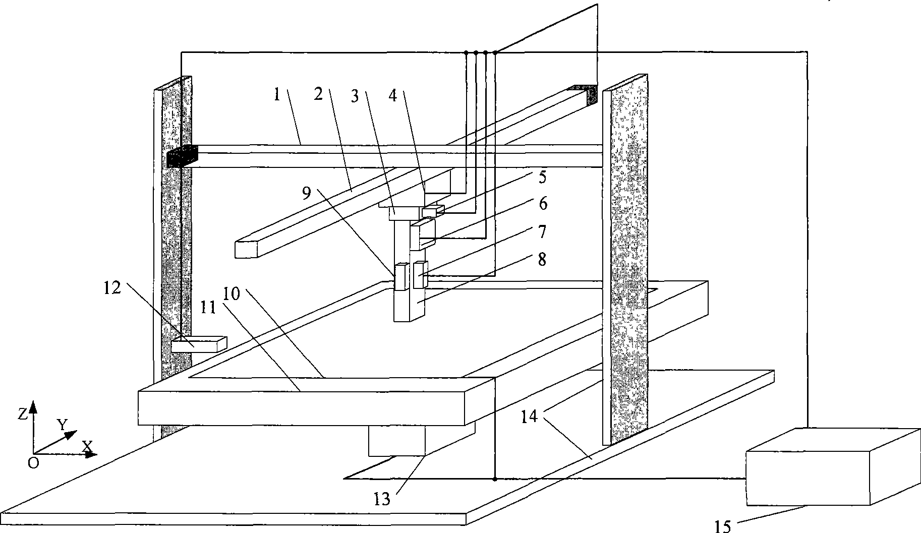
[0053] This solution prints fine interconnected metal wires by direct printing of metal ink, and uses fine interconnected metal wires to electrically connect the 3*4 CMOS active pixel image sensor module arrays on the substrate to form a complete flat panel detection device. The substrate composed of multiple CMOS active pixel image sensor modules is not flat, each CMOS active pixel image sensor and solder joints are higher than the surface of the substrate, and there is a gap between the image sensor and the image sensor, so that There will be a groove (that is, the modules on the entire substrate form a step), and the existing inkjet printing device that can only print patterns on a flat surface can no longer meet the requirements, so a design suitable for this program is designed. Printing device and printing method.

[0054] First, the inkjet printing printing device is designed in a clean cabinet to ensure that the surface of the module to be printed is clean so that the...

no. 2 example

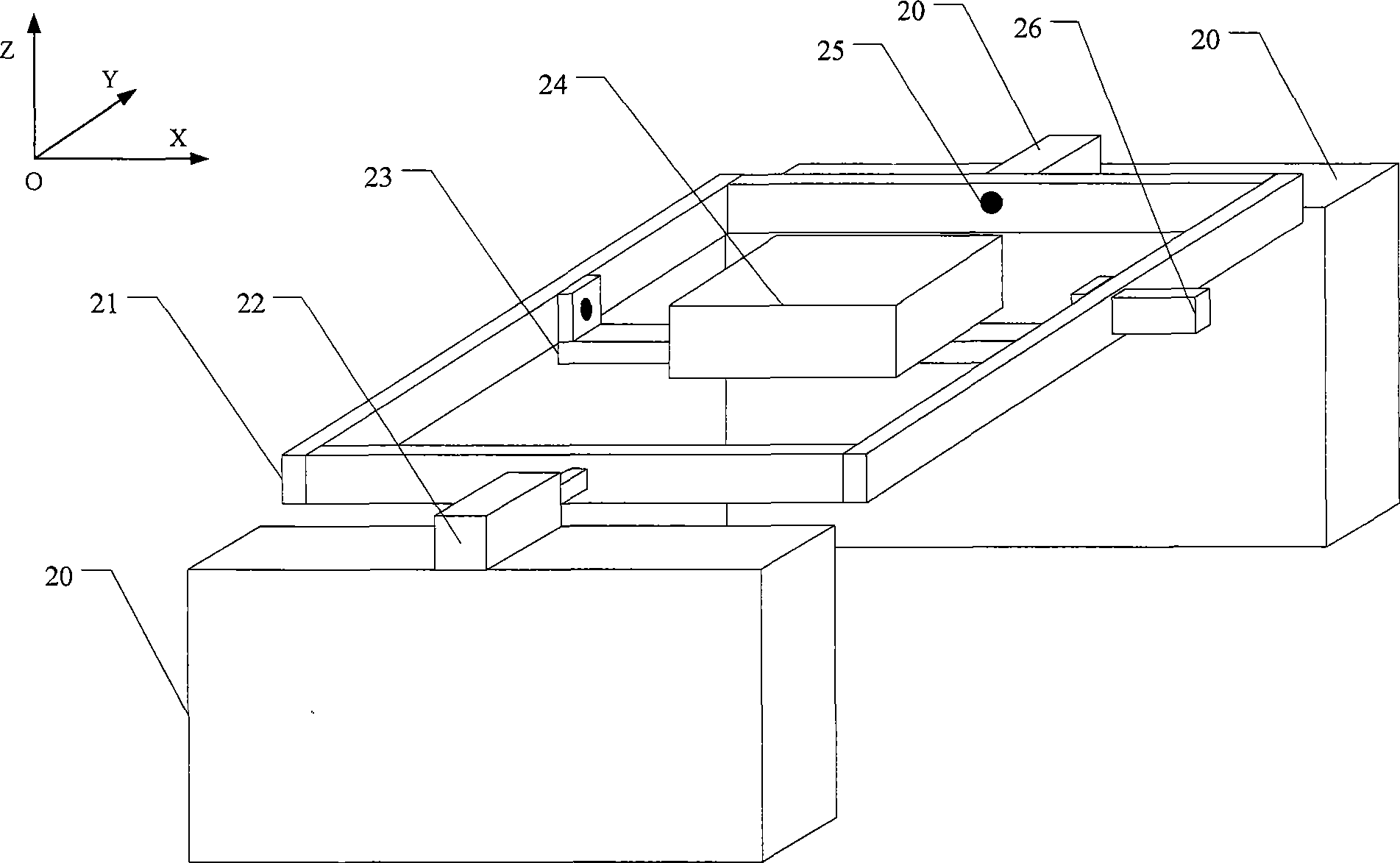
[0101] In this embodiment, the pattern of fine interconnected metal wires is printed by direct printing of metal ink, and a plurality of pre-encapsulated IC chip modules or encapsulated chips on the substrate are electrically connected to each other with fine interconnected metal wires to replace The traditional metal wire connection and PCB copper cladding process greatly reduce the cost of processing and increase the flexibility of interconnection.

[0102] also adopted figure 1 The printing device of inkjet printing is an application example of making interconnection wires on a substrate fixed with multiple electronic components, and connecting independent units into a complete electronic device. Since the solder joints of the electronic chips on the substrate will be on the On the surface, the wiring path printed in this way will pass through the vertical surface of the steps. In order to print high-quality metal wires under such circumstances, a high-precision platform is...


PUM


Abstract

The invention relates to a printing device, which can perform precise conductive pattern printing on a step shaped substrate, and comprises a platform module, a printing module, and a head movement module, wherein at least one of the platform module and the head movement module is provided with a rotating movement unit, and the rotating movement unit can drive a platform or a head to rotate around an X axis and a Y axis respectively, thereby ensuring that the head aligns a step surface which has an angle a with an X-Y plane to print; and the angle a is an angle which is more than 0 degree and is less than or equal to 90 degrees. A main innovation point is that the printing device can continuously print on the step shaped substrate; and the rotating movement unit is arranged on the printing device, or a step of real-time rotating printing of the head is added in a printing method, or the printing is respectively performed in a horizontal plane and a step plane, so as to solve the continuous problem of physical property of a metal conducting wire printed on the surface of the step shaped substrate, and ensure that the printed metal wire is not interrupted and has good electrical conductivity.

Description

technical field [0001] The present invention relates to a printing device and printing method for printing fine conductive patterns, in particular to a device for inkjet printing fine interconnection metal lines on uneven substrates composed of multiple electronic modules in the field of multi-chip packaging or integration and methods. Background technique [0002] In the process of electronic processing (especially microelectronics) or multi-chip packaging, metal wiring technology is the basis for interconnecting components on the substrate and transmitting signals to construct a complete system. It is also an indispensable process step in the preparation of various electronic devices. [0003] At present, the metal wiring in electronic devices is usually processed by first processing a flat plate (PCB board) with a metal wire pattern, and then fixing the electronic components on the flat plate by welding. In this way, the following steps are required-designing circuit dia...

Claims


Application Information

Patent Timeline
Patent Type & Authority Applications(China)
IPC IPC(8): B41J3/407B41J25/308B41J29/393B41J2/01H05K3/10H01L21/60H01L21/48
CPCH01L24/25H01L24/82H01L24/24H01L2224/24H01L2224/25H01L2924/15788
Inventor 刘建强范波高鹏苗新利郭涛
Owner CARERAY DIGITAL MEDICAL TECH CO LTD
Why Eureka
Try Eureka