Press-key backlight light-guiding film and its production method
A production method and technology of light guide film, which are applied in the direction of light guide, light guide of lighting system, optics, etc., can solve the problems such as the inability to use light guide film for transparent crystal button mobile phones, no specific requirements for transparency, and increase the utilization rate of backlight energy, etc. The effect of high yield, improved transparency and high production efficiency
- Summary
- Abstract
- Description
- Claims
- Application Information
AI Technical Summary
Problems solved by technology
Method used
Image
Examples
Embodiment 1
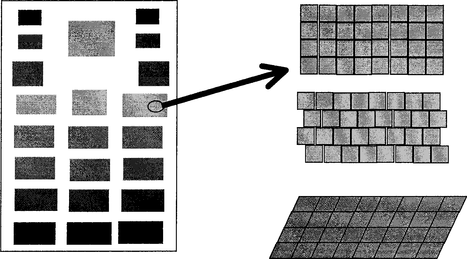
[0025] There are two main ways of dot arrangement in the existing light guide film, (1) the dots are arranged in a variable density; (2) the dots are arranged in a variable diameter; it can be seen that the dots in the above arrangement are discretely distributed, and after LED lighting, each Luminous dots will be clearly visible.
[0026] See attached figure 1 As shown, the adjacent light guide network points of the present embodiment are closely arranged, and the network point distribution diagram of a certain mobile phone button light guide film designed in this way is as follows figure 1 shown on the left. Because the network dots are closely arranged, each light guide area behaves as a continuous light-emitting surface. The dot depth of each area varies with the change of the LED luminous curve. The partial enlargement of which is as figure 1 shown on the right. figure 1 The upper part on the right is a schematic diagram of the regular arrangement of square dots; the...
Embodiment 2
[0028] Embodiment 2: The light guide film mold in Embodiment 1 can be made by laser photolithography. Coating photoresist, such as AZ glue or dry film, on the glass substrate with a coating thickness of 10um-20um.
[0029] The laser used can be a 405nm semiconductor laser or a 351nm DPSSL pulsed laser. For the 405nm laser, the exposure depth is controlled by controlling the exposure time; for the 351nm laser, the exposure depth is controlled by controlling the number of laser output pulses. Lithography depth range is usually 1-20um.
[0030] After the corresponding area is exposed and developed, a concave groove, that is, a light guide dot, is formed on the surface of the photoresist. After the production is completed, the electroforming process will be used to form a metal mold. Usually, metal nickel is selected as the mold material. The thickness of the electroformed nickel mold material is usually 50um-150um; it is suitable for flat pressing or roll-to-roll embossing in t...
Embodiment 3
[0031] Embodiment 3: The mold of the light guide film in Embodiment 1 can be made by laser direct etching. The base material of the mold can be PC or nickel, and the dot groove structure can be obtained by etching. After the production is completed, the electroforming process will be used to form a metal mold, and metal nickel is usually selected as the mold material.
[0032] The laser used may be a 527nm or 351nm DPSSL pulsed laser. The exposure depth is controlled by controlling the number of laser output pulses. The etching depth is usually in the range of 1-20um.
[0033] The etched mold is a concave mold, and after electroforming, a convex mold can be obtained.
[0034] The thickness of the electroformed nickel mold material is usually 50um-150um; it is suitable for the mass production of light guide film by flat pressing or roll-to-roll embossing in the subsequent process. The light guide film material is usually PC, and the thickness can be 100um; 125um; 254um; 381...
PUM
 Abstract
Description
Claims
Application Information

