Device and method for forming a three-dimensional circuit board
A technology of three-dimensional circuit board and circuit board, which is applied in the direction of printed circuit, printed circuit manufacturing, electrical recording process using charge pattern, etc., can solve the problem of end warping of circuit board, and achieve the effect of suppressing end warping
- Summary
- Abstract
- Description
- Claims
- Application Information
AI Technical Summary
Problems solved by technology
Method used
Image

Examples
Embodiment 1
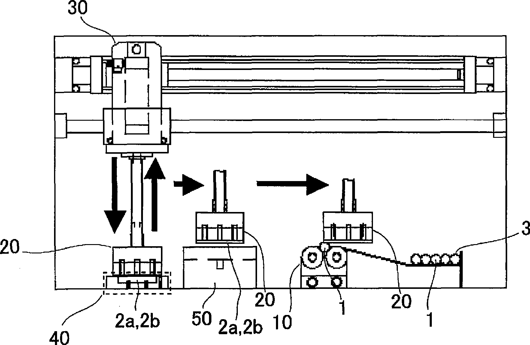
[0049] First, the circuit board 2b is produced as follows.
[0050] Using a 35 μm thick PET film (manufactured by Toyobo Co., Ltd., A4100), a copper thin film was formed on the surface by a sputtering method, and then a copper layer was formed by an electrolytic copper plating method. For electrolytic copper plating, use an electroplating solution with a copper sulfate concentration of 90g / liter and a sulfuric acid concentration of 180g / liter at room temperature, by making the cathode current density 2A / dm 2 , forming a copper capping layer with a thickness of 8 μm.
[0051] Furthermore, a dry film resist (dry film resist) (manufactured by Asahi Kasei Co., Ltd., AQ-1158) was pasted on the surface of the copper layer by a photolithography resist method, and a mask having a predetermined wiring shape was used to apply a dry film resist on the surface of the copper layer. Exposure is carried out on the agent, and then development, etching, and stripping of the dry film resist ar...
Embodiment 2
[0064] First, the circuit board 2 is fabricated as follows.
[0065] Using a double-layer substrate (manufactured by Sumitomo Metal Mining Co., Ltd., S'perFlex) in which a 38-μm-thick polyimide film is laminated with an 8-μm-thick copper foil, it is pasted on the surface of the copper layer by a photoresist method. Dry film resist (manufactured by Asahi Kasei Co., Ltd., AQ-1158), make a mask of the wiring shape, after that, expose on the dry film resist, then develop, etch and peel off the dry film resist to obtain Circuit board 2b.
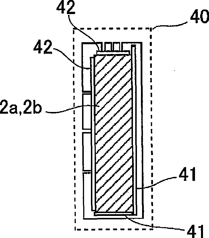
[0066] Next, the obtained circuit board 2b and the thermocompression-bonding type adhesive film 2a with a separator (manufactured by Nikon Industry Co., Ltd., SAFW) were each cut with a die and rotated. The side in the axial direction is 50.3 mm, and the side in the perpendicular direction is 350 mm. In addition, in this adhesive film 2a, the separator is arrange|positioned only on the surface side. After cutting, the adhesive film with the se...
Embodiment 3
[0075] As the roll 1 , an aluminum pipe having an adhesive layer formed on its surface was used. Specifically, a solution obtained by diluting a solution-type denatured epoxy-based adhesive (Aron mighty AS-60, manufactured by Toagosei Co., Ltd.) with toluene in advance to 2 times was used. For a diameter of 16 mm, An aluminum tube with a length of 300 mm was dip-coated, heated to 100° C., and kept for 2 minutes. The dried aluminum tube was used as the roll 1. The process was the same as in Example 2 except that the process of sticking the adhesive film 2 a was omitted. , the roller 1 is heated with a heater by a rotating device, and the adhesive layer is pasted on the circuit board 2b in an activated state, thereby obtaining a three-dimensional circuit board 3 .
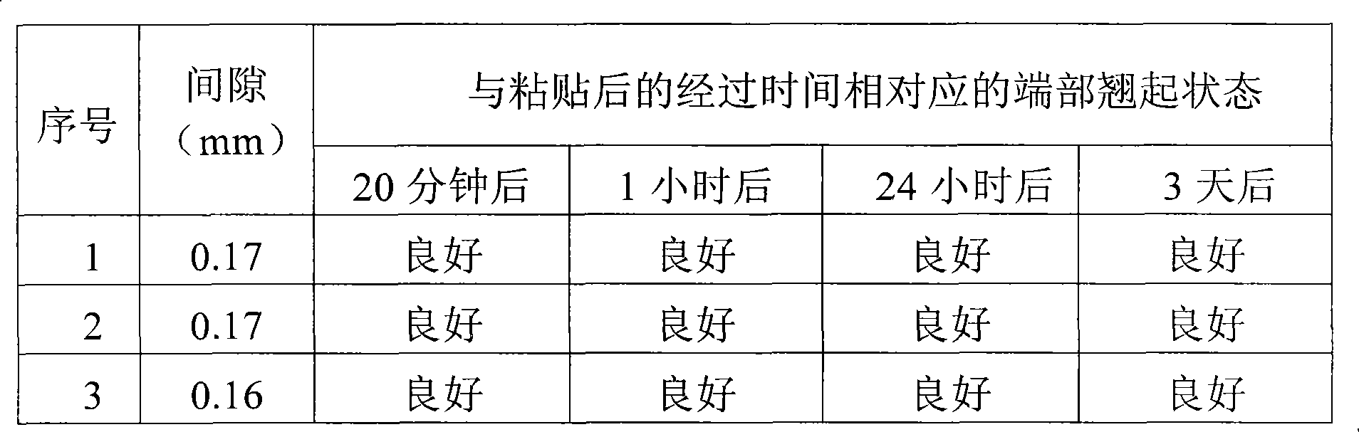
[0076] From the obtained three-dimensional wiring board 3 , the gap between the sides of the pasted wiring board 2 b was measured for each sample. In addition, the state of curling up of the end according to the ela...
PUM
 Abstract
Description
Claims
Application Information
 - R&D
- Intellectual Property
- Life Sciences
- Materials
- Tech Scout
- Unparalleled Data Quality
- Higher Quality Content
- 60% Fewer Hallucinations
Browse by: Latest US Patents, China's latest patents, Technical Efficacy Thesaurus, Application Domain, Technology Topic, Popular Technical Reports.
© 2025 PatSnap. All rights reserved.Legal|Privacy policy|Modern Slavery Act Transparency Statement|Sitemap|About US| Contact US: help@patsnap.com