Solder ball printing device

A technology for printing devices and solder balls, which is applied to tin feeding devices, auxiliary devices, assembling printed circuits with electrical components, etc., can solve the problems of increased production tact, increased cost of bump formation, and poor productivity, and improved operating efficiency. , The effect of improving filling efficiency and reducing equipment cost

Inactive Publication Date: 2009-07-29
HITACHI LTD
View PDF2 Cites 13 Cited by
  • Summary
  • Abstract
  • Description
  • Claims
  • Application Information

AI Technical Summary

Problems solved by technology

However, since the printing method is difficult to ensure the uniformity of the transfer volume, the solder bumps after reflow are pressed by flattening and the height is smoothed, so there are problems in the number of steps and high equipment costs.
In addition, in the case of finerization such as 100 to 150 μm pitch along with the high density of devices, there are problems of poor printing yield and poor productivity.
[0009] On the other hand, the solder ball transfer method can form highly stable bumps by ensuring the classification accuracy of the solder balls. In the case of increased production tact, there is a problem that the cost of bump formation increases due to the increase in jig/equipment prices
[0010] In addition, in the method of shaking or vibrating the screen of Pa

Method used


Image

  • Solder ball printing device
  • Solder ball printing device
  • Solder ball printing device

Examples


Example Embodiment

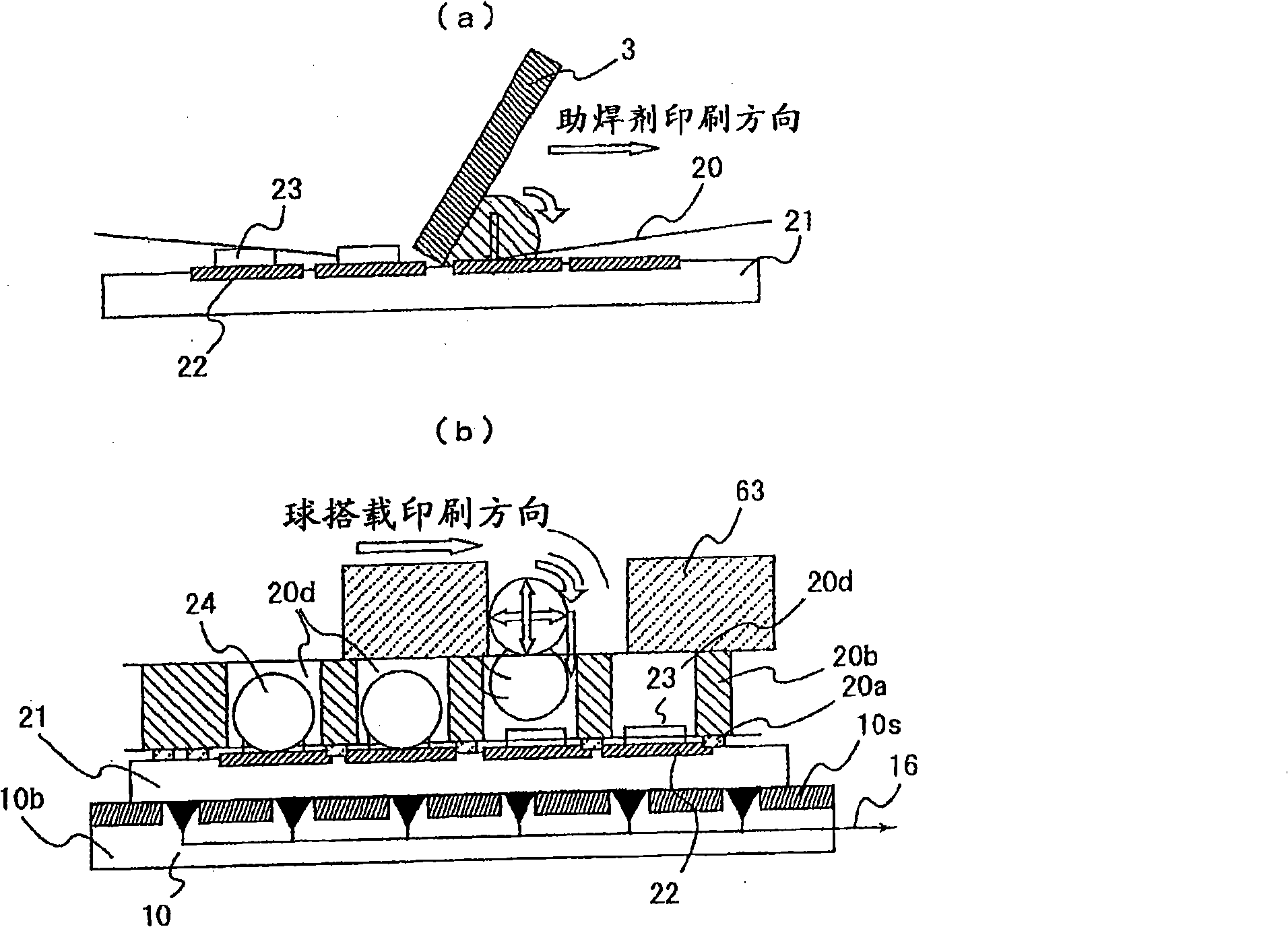
[0037] Hereinafter, preferred embodiments of the printing apparatus and bump forming method of the present invention will be described with reference to the drawings. figure 1 Shows the outline of the printing process in the flux printing section and the solder ball filling / printing section. figure 1 (a) shows the flux printing process, (b) shows the state of solder ball filling / printing.

[0038] in figure 1 In (a), the flux is placed on the flux printing screen 20 with openings provided in accordance with the position and shape of the electrode pads 22 provided on the substrate 21 in advance, and the squeegee 3 is moved. A predetermined amount of flux 23 is printed on the electrode pad 22 of the substrate 21.

[0039] In this embodiment, the screen 20 is a screen for flux printing, and a metal screen made by an additive method is used to ensure high-precision pattern position accuracy. As the scraper 3, any one of a square scraper, a sword scraper, or a flat scraper is used. ...


PUM

PropertyMeasurementUnit
Surface flux densityaaaaaaaaaa

Abstract

The invention provides a solder ball printing device, which can efficiently and reliably fill/print solder ball, and form a bump. The solder ball printing device of the invention comprises a flux printing part for printing flux on an electrode pad of a substrate; a solder ball filling/printing part for providing solder ball on the electrode printed with the flux; and a check/repair part for checking the condition of the substrate printed with the solder ball and repairing according to bad condition. A flux checking/repairing part, for checking the condition of the substrate printed with the flux and repairing according to bad condition, is arranged between the flux printing part and the solder ball filling/printing part, while the solder ball filling/printing part comprises a printing unit having a mesh for providing solder ball for the substrate and a slit-like body for filling solder ball to the mesh.

Description

technical field [0001] The invention relates to a screen printing device, in particular to a solder ball printing device for printing solder balls on the surface of a substrate. Background technique [0002] In the formation of spherical bumps (50 μm to 100 μm in diameter) with a pitch of 100 to 180 μm, there is a printing method in which solder paste is printed and then reflowed to form solder balls using a known high-precision screen printing device. As an example of a screen printing apparatus, it includes: a substrate carrying in conveyor, a substrate carrying out conveyor, a table with a lifting mechanism, a mask with a transfer pattern as an opening, a squeegee, a squeegee lifting mechanism, and The scraper head of the horizontal movement device, and the control device for controlling these parts. [0003] After the substrate is carried into the device from the carry-in conveyor part, the substrate is temporarily positioned and fixed on the printing table part, and th...

Claims


Application Information

Patent Timeline
IPC IPC(8): H01L21/60H01L21/66H05K3/34B23K3/00B23K3/06
CPCH01L2224/11005H01L2224/742B23K3/08H05K3/34H05K13/04
Inventor 本间真向井范昭川边伸一郎五十岚章雄
Owner HITACHI LTD
Why Eureka
Try Eureka