
Two-body type base semiconductor laser

A technology of semiconductors and lasers, applied in the field of lasers, can solve the problems of large tracking errors of lasers, degradation of optical isolation of lasers, and high assembly costs

Inactive Publication Date: 2009-07-29
大连艾科科技开发有限公司
View PDF0 Cites 3 Cited by
  • Summary
  • Abstract
  • Description
  • Claims
  • Application Information

AI Technical Summary

Problems solved by technology

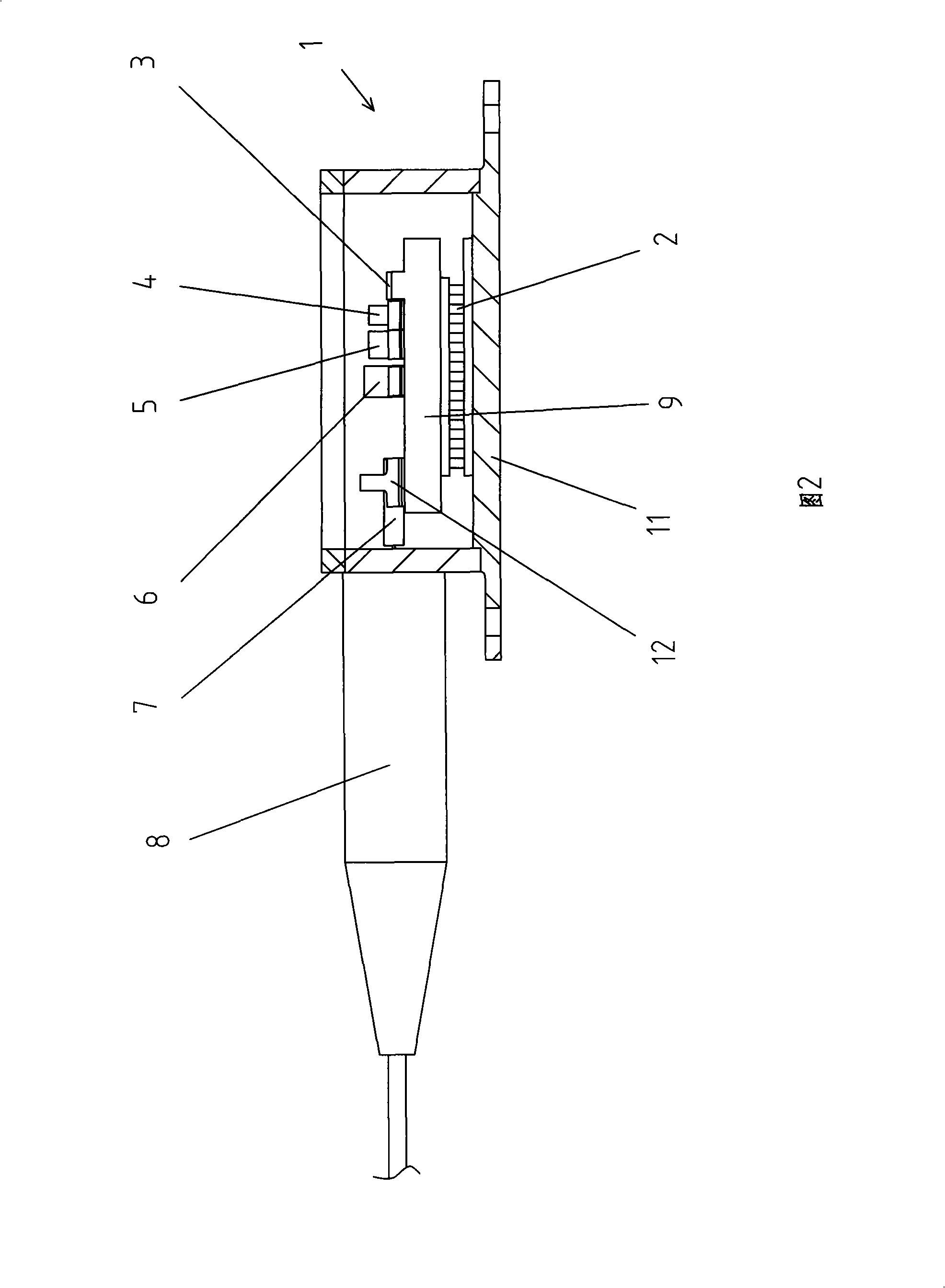
[0005] One kind of LD heat sink and optical component integrated base structure (as shown in Figure 2), its disadvantage is: because the base 9 carries all the optical coupling elements (including the laser diode 3 (LD) heat sink) First lens 4, optical isolator 5, second lens 6, optical fiber 7), so base 9 must be done big enough
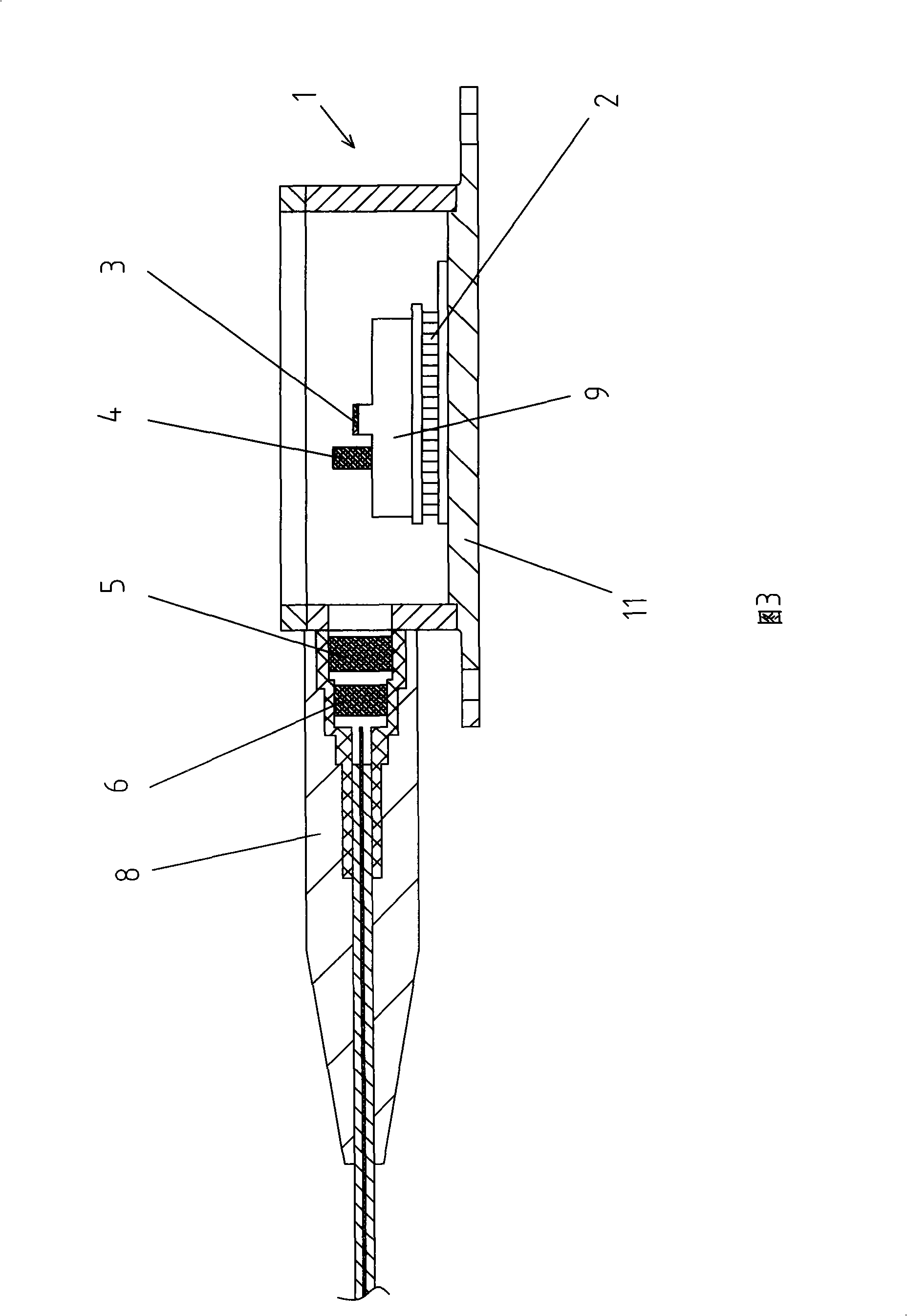
The disadvantage is that the second optical coupling lens and the isolator are installed on the window tube of the housing, and the window tube will tilt under high temperature due to thermal expansion and contraction of the housing material
As a result, the shell body is tilted, which causes the axis of the isolator and the second lens installed on the window tube to tilt (as shown in Figure 4), resulting in changes in the optical coupling efficiency of the laser and changes in the output power.
Therefore, at high temperature (such as when the shell temperature reaches 85°C), although the TEC can still work normally, the tracking error of the laser will become very large, and the output power will change beyond the specified standard.
In addition, since the isolation is not temperature-controlled, the optical isolation of the laser will also deteriorate at high temperatures, unless a Class 2 optical isolator with good temperature characteristics is used
But this also greatly increases the cost
In addition, the assembly of this structure requires more than two laser welding machines, and the assembly cost is relatively high

Method used


Image

  • Two-body type base semiconductor laser
  • Two-body type base semiconductor laser
  • Two-body type base semiconductor laser

Examples


Embodiment Construction

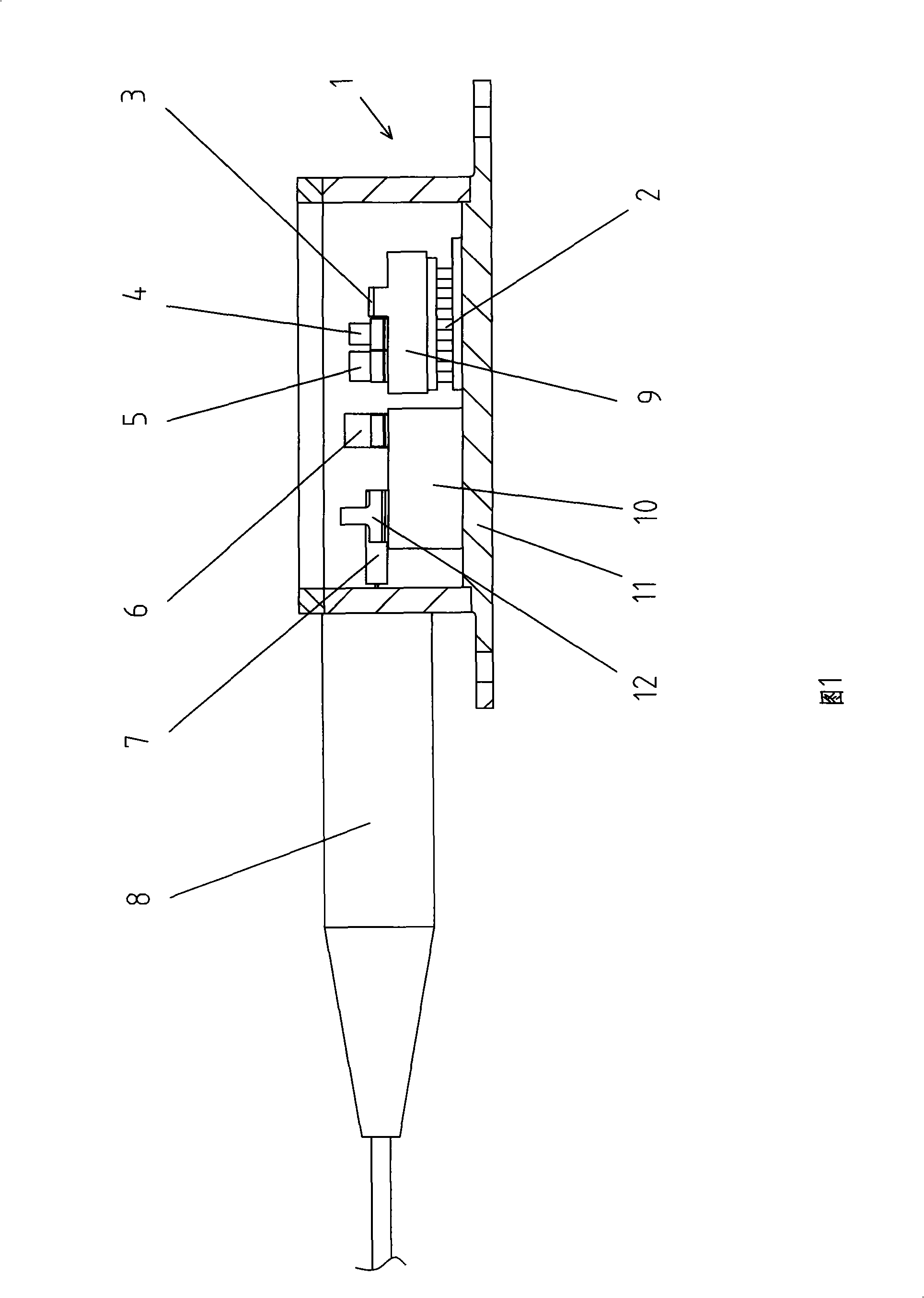
[0015] As shown in Figure 1: 1 is the shell, the shell bottom 11 of the shell 1 is made of tungsten copper material, and the other parts are made of Kovar material. A semiconductor refrigerator (TEC) 2 is provided inside the housing 1 , a first base 9 is provided above the semiconductor refrigerator 2 , and a second base 10 is directly provided on the bottom 11 of the housing. The laser diode (LD) 3 and the first lens 4 are arranged on the first base 9, and the optical isolator 5, the second lens 6, and the optical fiber 7 can be respectively arranged on the 9 and 10 according to the actual situation. The general structure is that a laser diode (LD) 3, a first lens 4 and an optical isolator 5 are arranged on a first base 9, and a second lens 6 and an optical fiber 7 are arranged on a second base 10 (as shown in FIG. 1 ). The end of the optical fiber 7 is fixed by a saddle-shaped optical fiber holder 12 . 8 is a window tube connected with the housing 1, and the inner center l...


PUM


Abstract

The invention relates to a laser, in particular to a two-body type base semiconductor laser, which includes a shell (1). A semiconductor freezer, a base, as well as a laser diode, a first lens, an optoisolator, a second lens and a fiber arranged on the base, are arranged in the shell (1). The laser is characterized in that the base is of a two-body structure consisting of a first base (9) and a second base (10); the laser diode is arranged on the first base (9); and the semiconductor freezer is arranged below the first base (9). The semiconductor laser has the advantages of reduced passive thermal load and energy consumption of the semiconductor freezer, improved thermal performance, good stability, low cost and convenient installation.

Description

technical field [0001] The invention relates to a laser, in particular to a two-body base semiconductor laser. Background technique [0002] At present, users of semiconductor lasers for communication have higher and higher requirements for high-temperature thermal characteristics of lasers. On the one hand, the highest voltage provided by the user's circuit board to the semiconductor cooler (TEC) cannot exceed 2.6V, and the current cannot exceed 1.2A. . On the other hand, users often require that the laser can work until the actual temperature of the tube and shell is as high as 85°C. If the thermal load of the semiconductor laser is too large, when the shell temperature of the laser reaches 85°C, the voltage of the TEC will be much higher than 2.6V, and at this time the board cannot normally supply enough current to the TEC. Therefore, the TEC cannot normally pump the heat of its cooling end, and finally cannot stabilize the temperature of the laser diode (LD) and its he...

Claims


Application Information

Patent Timeline
IPC IPC(8): H01S5/00H01S5/022H01S5/024H01S5/026H01S5/02G02B6/26
Inventor 张耐
Owner 大连艾科科技开发有限公司
Learn More