Electric power converter

A power conversion device and package technology, which is applied to circuit thermal devices, output power conversion devices, circuits, etc., can solve the problems of thermal damage to components, low heat-resistant temperature, and elevated temperature, and achieve miniaturization, reduction, and simplification. Support structure, cost reduction effect

Inactive Publication Date: 2009-07-29
DAIKIN IND LTD
View PDF1 Cites 6 Cited by
  • Summary
  • Abstract
  • Description
  • Claims
  • Application Information

AI Technical Summary

Problems solved by technology

[0007] However, by using such a wide bandgap semiconductor as described above, an element capable of high-temperature operation can be realized, but in this case, peripheral components such as a driver and a CPU need to be provided around the element, and the miniaturization of the element formed of the wide bandgap semiconductor is difficult. If the temperature is raised, these peripheral parts with relatively low heat-resistant temperature may be damaged by heat
[0008] For this reason, even if the above-mentioned wide bandgap semiconductor is used to form an element, there is a problem that it is substantially impossible to operate at a high temperature due to the restriction of the temperature rise of peripheral components.

Method used


Image

  • Electric power converter
  • Electric power converter
  • Electric power converter

Examples


Embodiment approach 1

[0096] -Overall composition-

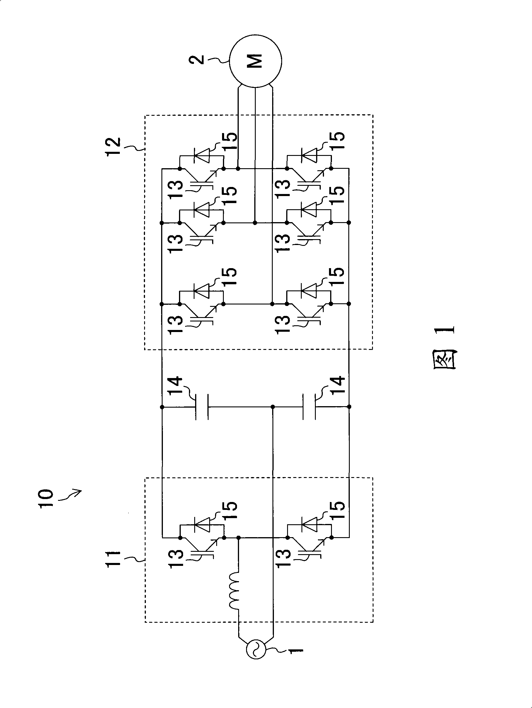
[0097] FIG. 1 shows an example of a circuit of a power conversion device 10 according to Embodiment 1 of the present invention. This power conversion device 10 includes a converter 11 for converting an AC voltage into a DC voltage, and an inverter 12 for converting the DC voltage converted by the converter 11 into a three-phase AC voltage. The converter 11 is connected to To the AC power source 1, the inverter 12 is connected to the motor 2 as a load.

[0098] The above-mentioned converter 11 and the inverter 12 have a plurality of main switching elements 13, 13, ..., and rectification from AC voltage to DC voltage is performed on the above-mentioned converter 11 by switching operations of the main switching elements 13, 13, .... Operation and power conversion operation of converting DC voltage to three-phase AC voltage on the above-mentioned converter 12 .

[0099] In addition, in the power conversion device 10, the two capacitors 14, 14 for s...

Embodiment approach 2

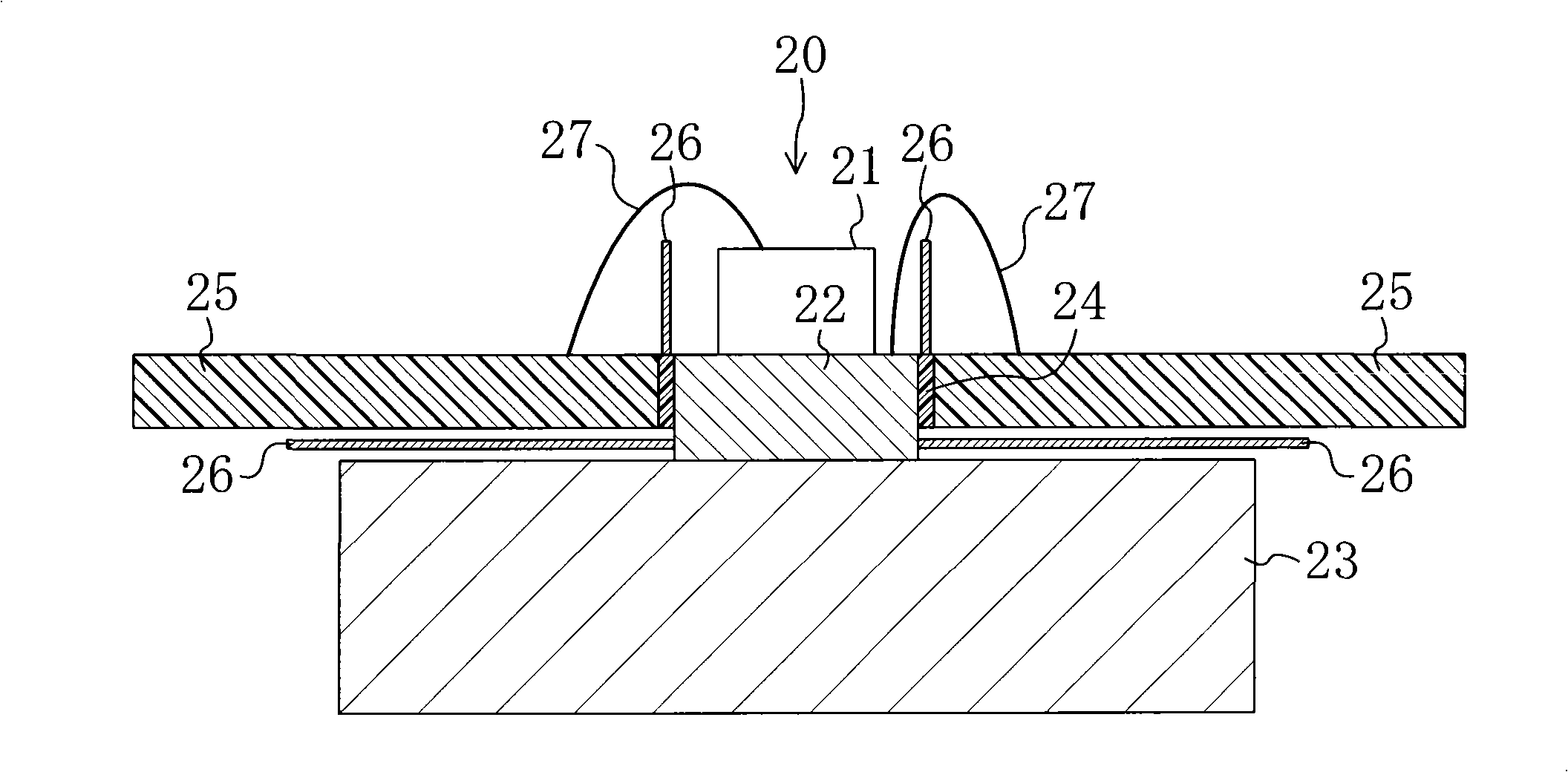
[0121] This second embodiment is different from the above-mentioned first embodiment in that the package 41 in which the chip 21 is sealed is not thermally insulated inside, but heat conduction to the substrate 42 side is suppressed externally.

[0122] In detail, such as Figure 4 As shown, a package 41 encapsulating a chip formed of a wide bandgap semiconductor such as silicon carbide (SiC) is connected to a printed circuit board 43 made of resin, for example, through a plurality of terminals 42, 42, . . . . In more detail, the surface of the above-mentioned printed substrate 43 ( image 3 In the lower surface), a pattern 44 is formed on which the above-mentioned terminals 42, 42, . . . are electrically connected.

[0123] On the other hand, in the package 41, a heat sink 45 is provided on the side opposite to the printed circuit board 43, and the heat sink 45 is configured to dissipate heat from the sealed package 41 of the chip.

[0124] And, the terminals 42, 42, ... of t...

Embodiment approach 3

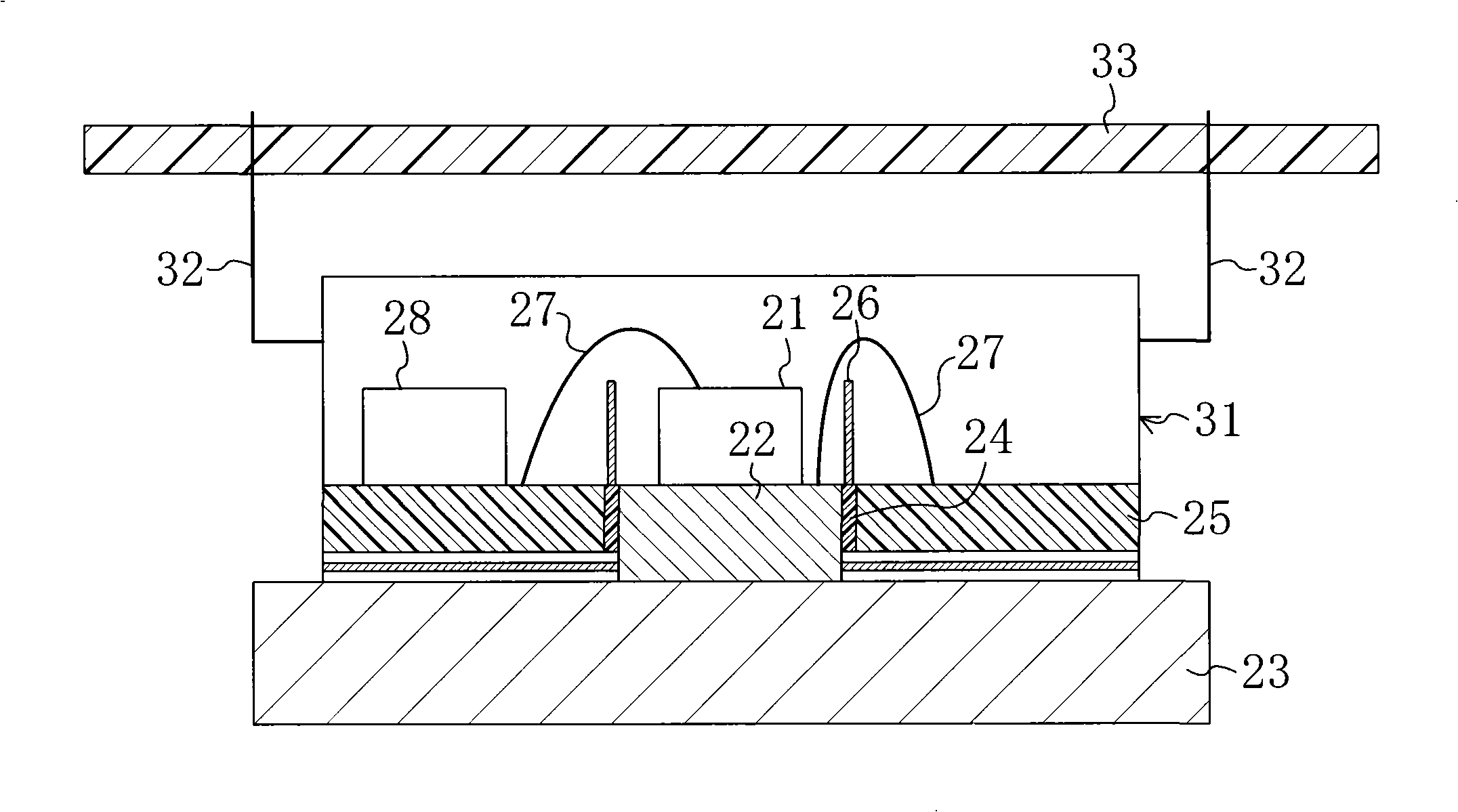
[0136] This Embodiment 3 is different from the above-mentioned Embodiment 2 in that the package body 41 is not directly assembled on the printed circuit board 43 , but is connected to the low heat-resistant Sexual printed substrate 53. Also, the same configurations as those in the above-mentioned second embodiment are denoted by the same reference numerals, and only different parts will be described.

[0137] Specifically, as Figure 5 As shown, a package 41 encapsulating a chip of a wide bandgap semiconductor such as silicon carbide (SiC) is mounted on a highly heat resistant printed circuit board 51 having a heat resistance temperature higher than the temperature at which the wide bandgap semiconductor can operate. Such a highly heat-resistant printed circuit board 51 is, for example, a highly heat-resistant resin or a metal substrate.

[0138] Furthermore, the high heat-resistant printed circuit board 51 assembled with the above-mentioned package 41 is connected to the lo...


PUM


Abstract

In the case where a chip is made of wide band gap semiconductor, a power conversion apparatus is obtained in which a component having a low heat resistant temperature is prevented from receiving thermal damage by heat generated at the chip. In a configuration including: a chip portion (20) including a chip (21) made of wide band gap semiconductor and a member (22, 23) having a heat resistant temperature equal to or higher than that of the chip (21); and a peripheral component (25) arranged in the vicinity of the chip portion (20) and having a heat resistant temperature lower than that of the chip (21). The chip (21) and the peripheral component (25) are thermally insulated from each other so that the temperature of the peripheral component (25) does not exceed the heat resistant temperature of the peripheral component (25).

Description

technical field [0001] The present invention relates to an inverter for converting a DC voltage into an AC voltage and a power conversion device for a converter for converting an AC voltage into a DC voltage. Background technique [0002] Hitherto, a power conversion device of an inverter for converting a DC voltage to an AC voltage and a converter for converting an AC voltage into a DC voltage has a plurality of switching elements as disclosed in Patent Document 1 Devices for performing power conversion actions are known. In addition, the above-mentioned Patent Document 1 discloses that since an element made of SiC semiconductor is used as the main switching element, the carrier frequency of PWM control can be increased, and the efficiency can be improved compared with the conventional configuration. [0003] In wide hand gap semiconductors such as silicon carbide (SiC) semiconductors mentioned above, since the dielectric breakdown electric field is about 10 times higher t...

Claims


Application Information

Patent Timeline
Patent Type & Authority Applications(China)
IPC IPC(8): H01L25/07H01L23/34H01L25/18H02M1/00
CPCH05K2201/09972H05K1/0201H05K2201/10022H05K1/0204H01L2924/01082H01L25/16H01L2924/01004H01L2924/01002H01L2924/13091H05K1/141H01L2924/01029H01L2924/19041H01L2224/48091H05K1/18H01L2224/484H01L24/48H01L2224/4899H05K2203/081H01L2924/3011H05K2201/09263H01L2224/48227H01L2924/19107H01L23/647H01L2924/01005H01L2924/01033H01L2924/01006H01L25/072H01L2924/01078H05K2201/062H01L2924/01014H01L2924/13055H05K2201/10166H01L2924/01031H01L2924/07802H01L2924/15747H01L2924/00014H01L2924/181H01L2924/00H01L2224/45099H01L2924/00012H01L2224/85399H01L2224/05599
Inventor 关本守满芳贺仁榊原宪一川嶋玲二阿卜杜拉·梅基前田敏行
Owner DAIKIN IND LTD
Why Eureka
Try Eureka