

Touching control panel
A technology of a touch panel and a refractive index matching layer, applied in the field of touch panels that can increase light transmittance, can solve the problems of affecting display quality, transmittance and contrast reduction, etc., so as to improve display quality, reduce reflectivity, reduce Improve penetration and contrast
- Summary
- Abstract
- Description
- Claims
- Application Information
AI Technical Summary
Problems solved by technology
Method used
Image

Examples
no. 1 example
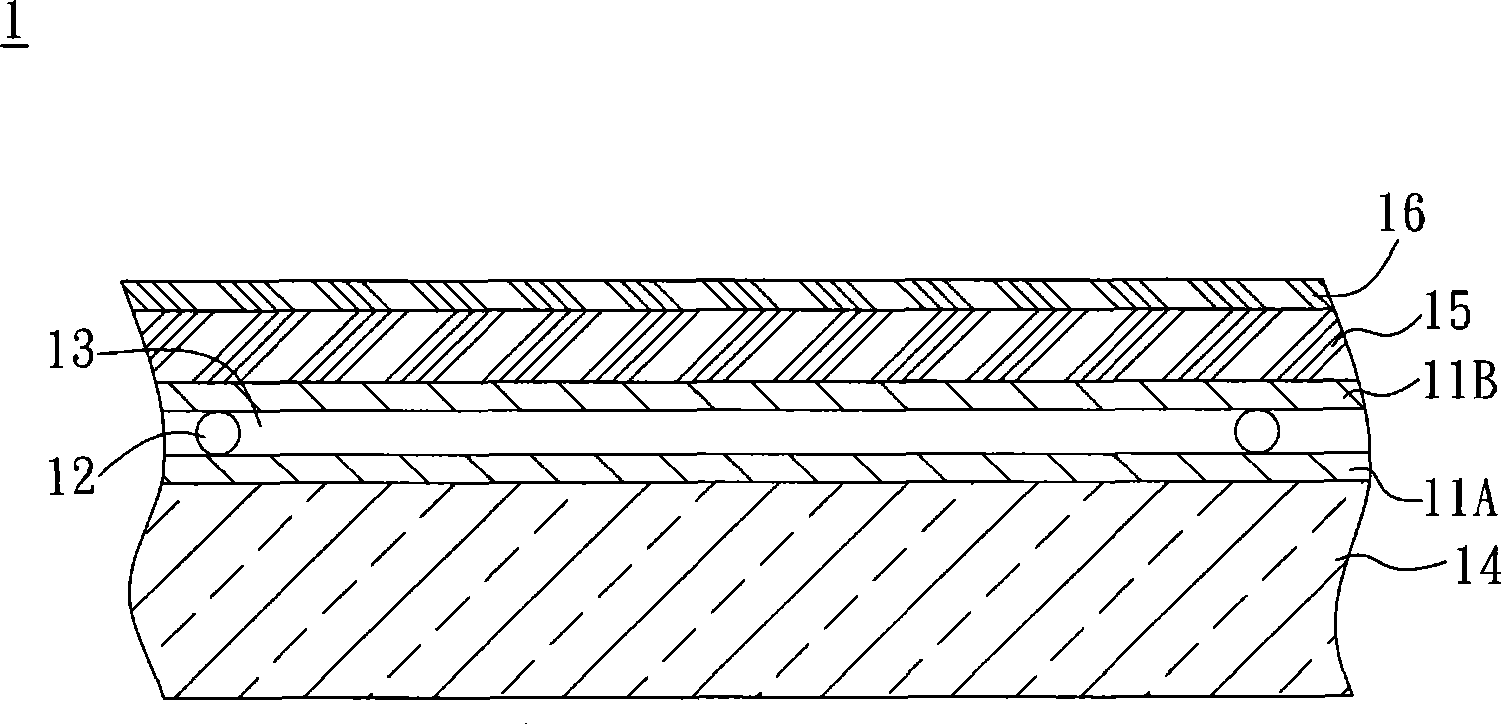
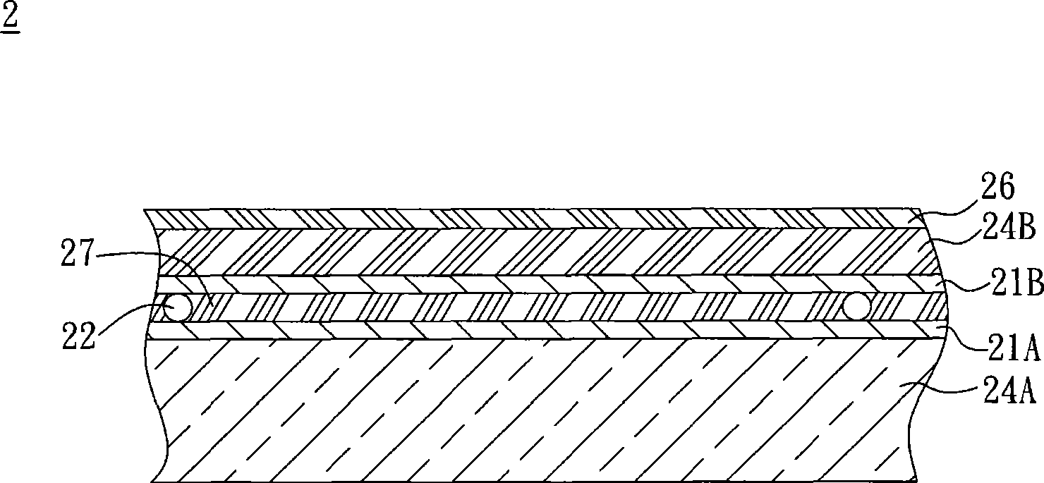
[0026] image 3 The touch panel 2 of the first embodiment of the present invention is shown. The touch panel 2 includes two transparent conductive films 21A, 21B and a refractive index matching layer 27 . The transparent conductive films 21A and 21B are arranged opposite to each other. The materials of the transparent conductive films 21A and 21B can be, for example but not limited to, indium tin oxide (ITO), indium zinc oxide (IZO), aluminum zinc oxide (AZO), gallium zinc oxide (GZO), zinc oxide (ZnO ), tin oxide or any combination thereof.
[0027] The refractive index matching layer 27 is disposed between the transparent conductive films 21A and 21B, and is an elastic insulating layer to replace the known air layer. The material of the refractive index matching layer 27 may include silicone, epoxy Or a combination thereof, the refractive index matching layer 27 can also be a liquid refractive index matching layer, and is preferably liquid silicone, liquid epoxy or a comb...
no. 2 example
[0034] Please refer to Figure 5 As shown, the touch panel 3 of the second embodiment of the present invention includes two transparent conductive films 21A, 21B and two refractive index matching layers 37A, 37B. The difference between the touch panel 3 and the touch panel 2 of the first embodiment is that the refractive index matching layers 37A and 37B are respectively located between the spacer 22 and the transparent conductive film 21A and between the spacer 22 and the transparent conductive film 21B. The object 22 is used to push against and separate the index matching layers 37A, 37B to form an air layer 38 . In addition, the refractive index matching layers 37A, 37B need to be conductive, and their materials may include transparent conductive materials, or a material with a lower refractive index mixed with transparent conductive materials and transparent dielectric materials. The transparent conductive material is, for example, indium tin oxide (ITO), indium zinc oxid...
no. 3 example
[0039] Please refer to Figure 7As shown, the touch panel 4 of the third embodiment of the present invention is similar to the above-mentioned second embodiment, but the difference is that the spacer 22 abuts and separates the first transparent conductive film 41A and the second transparent conductive film 41B, and refracts The index matching layer 47A is disposed between the transparent substrate 24A and the first transparent conductive film 41A, and the refractive index matching layer 47B is disposed between the transparent substrate 24B and the second transparent conductive film 41B. In terms of process, the refractive index matching layer 47A can be plated on the transparent substrate 24A simultaneously with the first transparent conductive film 41A, and the refractive index matching layer 47B can be plated on the transparent substrate 24B simultaneously with the second transparent conductive film 41B. The refractive index matching layers 47A and 47B can be a single layer ...
PUM
| Property | Measurement | Unit |
|---|---|---|
| refractive index | aaaaa | aaaaa |
| refractive index | aaaaa | aaaaa |
| refractive index | aaaaa | aaaaa |
Abstract
Description
Claims
Application Information