795nm quantum well laser based on AlGaAs/GaInP active region

An active region and quantum well technology, applied in the field of single quantum well semiconductor lasers, can solve the problems of undiscovered semiconductor laser technology, influence of laser reliability, unsatisfactory heat dissipation, etc., to improve maximum output power and reliability, improve photoelectricity Conversion efficiency, light absorption reduction effect

Active Publication Date: 2018-07-31
Shandong Huaguang Optoelectronics Co. Ltd.
View PDF3 Cites 4 Cited by
  • Summary
  • Abstract
  • Description
  • Claims
  • Application Information

AI Technical Summary

Problems solved by technology

However, in the field of quantum well lasers, no semiconductor laser technology with a wavelength output of 795nm has been found.
[0003] In addition, the epitaxial structure of existing quantum well lasers generally adopts a symmetrical structure centered on the active region, and the material components of the upper and lower confinement layers and the upper and lower wavegu

Method used


Image

  • 795nm quantum well laser based on AlGaAs/GaInP active region
  • 795nm quantum well laser based on AlGaAs/GaInP active region
  • 795nm quantum well laser based on AlGaAs/GaInP active region

Examples


Embodiment 1

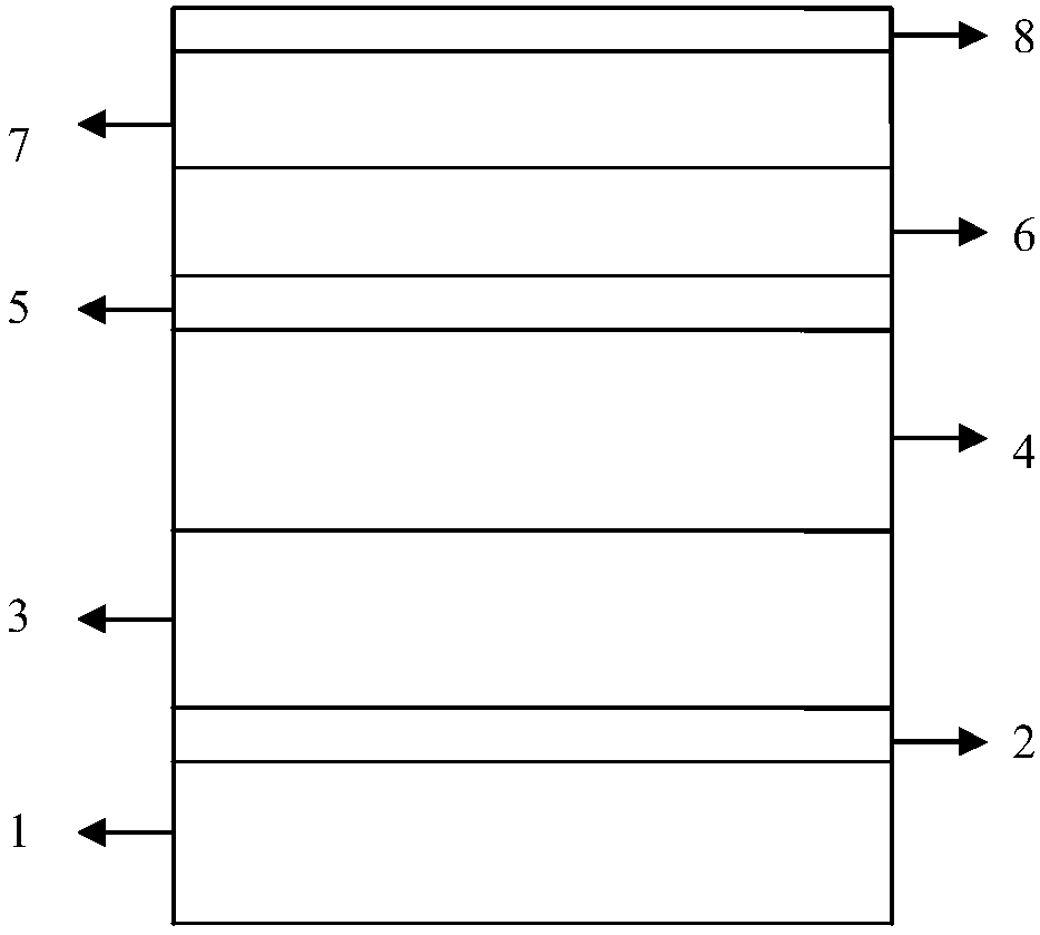
[0050] A 795nm quantum well laser based on AlGaAs / GaInP active region, the structure is as follows figure 1 As shown, from bottom to top are substrate 1 , buffer layer 2 , lower confinement layer 3 , lower waveguide layer 4 , quantum well layer 5 , upper waveguide layer 6 , upper confinement layer 7 and ohmic contact layer 8 .

[0051] Substrate 1: used for epitaxial growth of materials of various layers of the laser thereon, the substrate is an N-type highly doped gallium arsenic material with the (100) plane offset to the (110) direction, and the off angle is 15°. The doping concentration of N-type highly doped gallium arsenic is 2E18cm -3 .

[0052] The buffer layer 2 is grown on the substrate 1 with a doping concentration of 2E18cm -3 N-type highly doped gallium arsenic material with a thickness of 300nm.

[0053] The lower confinement layer 3 is made of N-type aluminum gallium indium phosphide material, grown on the buffer layer 2, with a doping concentration of 5E17cm...

Embodiment 2

[0062] Embodiment 2: A kind of AlGaAs / GaInP active region 795nm quantum well laser

[0063] As described in Example 1, the difference is:

[0064] Substrate 1 is an N-type highly doped gallium arsenic material with the (100) plane offset to the (110) direction, the off angle is 12°, and the doping concentration of the N type highly doped gallium arsenic is 3E18cm -3 .

[0065] Buffer layer 2: The doping concentration of N-type highly doped GaAs material is 2E18cm -3 , thickness 350nm.

[0066] Lower confinement layer 3: doping concentration of N-type aluminum gallium indium phosphide material 7E17cm -3 , thickness 1.1 μm. The aluminum content of the lower limiting layer was 15%.

[0067] The thickness of the lower waveguide layer 4 is 500nm, and the gallium indium phosphide layer with a thickness of 250nm near the lower confinement layer 3 is N-type doped with a doping concentration of 2E17cm -3 .

[0068] Quantum well layer 5: the thickness of AlGaAs is 8nm. When work...


PUM

PropertyMeasurementUnit
Thicknessaaaaaaaaaa
Thicknessaaaaaaaaaa
Thicknessaaaaaaaaaa

Abstract

The present invention provides a 795nm quantum well laser based on an AlGaAs/GaInP active region. The epitaxial structure comprises a substrate, a buffer layer, an N-type lower limit layer, a lower waveguide layer, a quantum well layer, an upper waveguide layer, and P-type upper limit layer and an ohmic contact layer from the bottom to the top. The upper waveguide layer and the lower waveguide layer are made of an aluminum-free material gallium indium phosphate, the quantum well layer is made of an aluminum gallium arsenide material, and a wide waveguide semi-aluminum-free active region is formed by the waveguide layers and the quantum well layer. According to the 795nm quantum well laser, the special requirements of a pump laser with the application of a small and simplified self-doubledlaser crystal can be satisfied, at the same time, the influence of the roughness of a growth interface and an episodic field at a cavity surface on the service and reliability of the laser can be reduced effectively by an optimized laser structure.

Description

technical field [0001] The invention relates to a high-efficiency and high-reliability 795nm strained quantum well laser, which belongs to the technical field of single quantum well semiconductor lasers. Background technique [0002] In recent years, rainbow holography, fine laser spectroscopy, and laser medicine have shown a strong demand for green lasers and dual-wavelength lasers. All solid-state lasers play an irreplaceable role in fine spectroscopy, detection, and laser medicine due to their advantages such as compact structure, high peak power, and narrow half-width of wavelength. Commonly used solid-state lasers are generally realized by a combination of semiconductor laser pump source, laser crystal, and frequency-doubling crystal. When realizing visible light laser (such as 532nm) output, it is necessary to adjust the laser crystal and frequency-doubling crystal to achieve the closest match. The process is complex and requires high requirements. . At the same time...

Claims


Application Information

Patent Timeline
IPC IPC(8): H01S5/34H01S5/343
Inventor 徐现刚李沛旭
Owner Shandong Huaguang Optoelectronics Co. Ltd.
Why Eureka
Try Eureka