Organic light emission diode and preparation method therefor

An electroluminescent device and luminescent technology, which is applied in the fields of electric solid-state devices, semiconductor/solid-state device manufacturing, electrical components, etc., can solve the problems of low light output and low light extraction efficiency

Inactive Publication Date: 2015-10-14
OCEANS KING LIGHTING SCI&TECH CO LTD +2
View PDF0 Cites 6 Cited by
  • Summary
  • Abstract
  • Description
  • Claims
  • Application Information

AI Technical Summary

Problems solved by technology

When light is transmitted from the anode to the substrate, total reflection is likely to occur at the interface between the anode and the substrate, and the light output is less, so that the light extraction efficiency is low

Method used


Image

  • Organic light emission diode and preparation method therefor
  • Organic light emission diode and preparation method therefor
  • Organic light emission diode and preparation method therefor

Examples


preparation example Construction

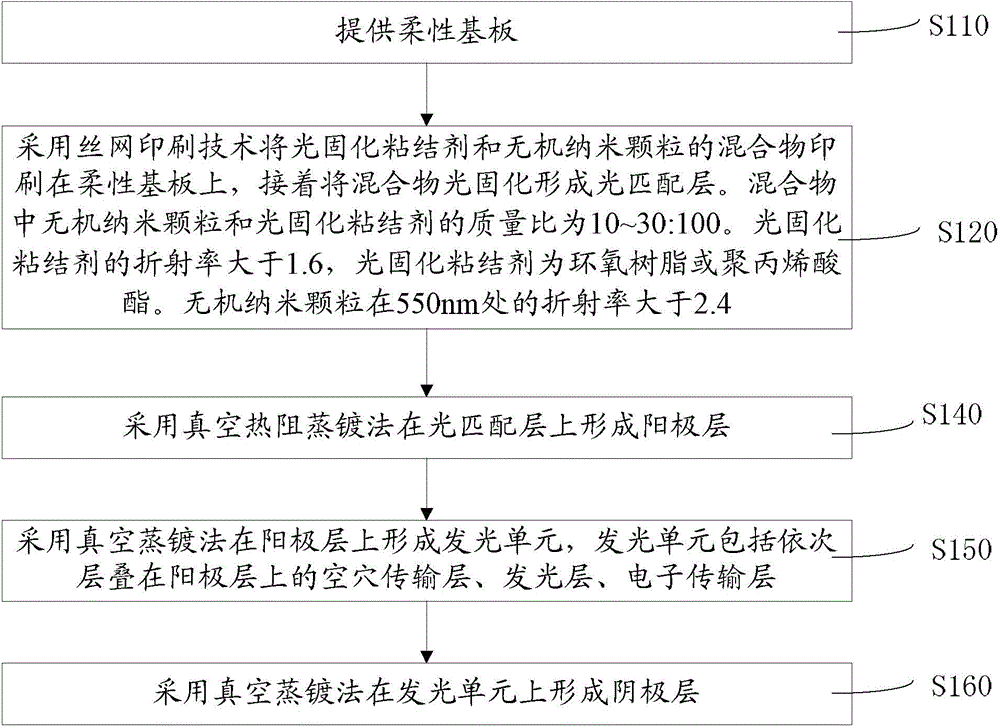
[0051] Such as figure 2 As shown, the preparation method of the above-mentioned organic electroluminescent device of one embodiment includes the following steps:

[0052] S110, providing a flexible substrate.

[0053] Flexible substrates are cleaned before use.

[0054] The flexible substrate can be a polymer transparent film. For example, polyethylene terephthalate (polyethylene terephthalate, PET) film, polyether sulfone resin (Poly (ether sulfones), PES) film, polycarbonate (Polycarbonate, PC) film or polyimide (Polyimide , PI) films, etc. The thickness of the flexible substrate may be 0.1mm˜0.5mm.

[0055] S120. Print the mixture of photocurable binder and inorganic nanoparticles on the flexible substrate by screen printing technology, and then photocure the mixture to form an optical matching layer. The mass ratio of the inorganic nanoparticles and the light-curing binder in the mixture is 10-30:100. The refractive index of the light-curing adhesive is greater than...

Embodiment 1

[0076] A PET substrate with a thickness of 0.1 mm is provided and cleaned.

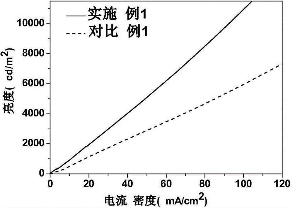
[0077] Mix PbS with epoxy resin at a mass ratio of 10:100. The particle size of PbS is 5 nm. Then ultrasonic vibration was dispersed for 1 hour to obtain a mixture. Then, the above mixture was printed on the surface of the flexible substrate by using screen printing technology with a mesh number of 1000 to form a film with a thickness of 20 μm. Then adopt photocuring method to cure the above thin film to form an optical matching layer.

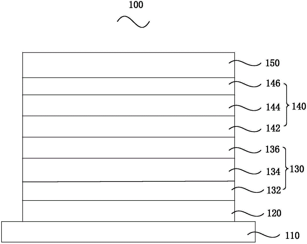
[0078] A first dielectric layer is formed on the optical matching layer by vacuum thermal resistance evaporation method. The material of the first dielectric layer is WO 3 , with a thickness of 40nm. A metal layer is formed on the first dielectric layer by vacuum thermal resistance evaporation method. The material of the metal layer is Ag, and the thickness is 18nm. A second dielectric layer is formed on the metal layer by vacuum thermal resistance evaporation ...

Embodiment 2

[0084] Provide a PES substrate with a thickness of 0.5mm and clean it.

[0085] Mix ZnS with polyacrylate at a mass ratio of 20:100. The particle diameter of ZnS is 25 nm. Then ultrasonic vibration was dispersed for 5 hours to obtain a mixture. Then, the above mixture was printed on the surface of the flexible substrate by using screen printing technology with a mesh number of 600 to form a film with a thickness of 100 μm. Then adopt photocuring method to cure the above thin film to form an optical matching layer.

[0086] A first dielectric layer is formed on the optical matching layer by vacuum thermal resistance evaporation method. The material of the first dielectric layer is MoO 3 layer with a thickness of 80 nm. A metal layer is formed on the first dielectric layer by vacuum thermal resistance evaporation method. The material of the metal layer is Al, and the thickness is 30nm. A second dielectric layer is formed on the metal layer by vacuum thermal resistance eva...


PUM

PropertyMeasurementUnit
thicknessaaaaaaaaaa
particle diameteraaaaaaaaaa
thicknessaaaaaaaaaa

Abstract

An organic light emission diode comprises a flexible substrate, a light matching layer, an anode layer, a light emitting unit and a cathode layer which are sequentially laminated. The material of the light matching layer is a mixture of inorganic nanometer particles and a light-cured binder with the mass ratio of 10-30:100. The refractive index of the light-cured binder is larger than 1.6 and is epoxy resin or polyacrylate, and the refractive index of the inorganic nanometer particles is larger than 2.4 at 550nm. According to the organic light emission diode, after the light-cured binder of the light matching layer is added with the inorganic nanometer particles of a higher refractive index, the refractive index of the light matching layer reaches 1.7-1.8. By arranging the light matching layer between the anode layer and the flexible substrate, the difference between refractive indexes of two layers of adjacent structures is reduced, so that the critical angle of total reflection is increased, the light output is increased, and the light extraction efficiency is improved. In addition, the invention provides a preparation method for the organic light emission diode.

Description

technical field [0001] The invention relates to the technical field of electroluminescence, in particular to an organic electroluminescence device and a preparation method thereof. Background technique [0002] Organic Light Emission Diode (OLED) has the characteristics of high brightness, wide range of material selection, low driving voltage, fully cured active luminescence, etc., and has the advantages of high definition, wide viewing angle, and fast response speed. A display technology and light source with great potential, in line with the development trend of mobile communication and information display in the information age, and the requirements of green lighting technology, is the focus of many researchers at home and abroad. [0003] Flexible OLED light-emitting devices have the advantages of flexibility and portability. However, there are also some problems in traditional OLED light-emitting devices. For example, OLEDs usually use Indium Tin Oxide (ITO) films as a...

Claims


Application Information

Patent Timeline
Patent Type & Authority Applications(China)
IPC IPC(8): H01L51/52H01L51/54H01L51/56
Inventor 周明杰冯小明张娟娟王平
Owner OCEANS KING LIGHTING SCI&TECH CO LTD
Why Eureka
Try Eureka