Single proton source for implementing electrical injection by photonic crystal microcavity and wafer linking technique

A technology of photonic crystal microcavity and single photon source, which is applied in the structure of optical resonant cavity, device for controlling laser output parameters, circuit, etc., can solve the problems of single photon source electric injection, etc., to improve emission efficiency and Q value , The effect of improving the total Q value

Inactive Publication Date: 2009-08-05
INST OF SEMICONDUCTORS - CHINESE ACAD OF SCI
View PDF0 Cites 33 Cited by
  • Summary
  • Abstract
  • Description
  • Claims
  • Application Information

AI Technical Summary

Problems solved by technology

[0008] In view of this, the main purpose of the present invention is to provide a single photon source that uses photonic crystal microcavity and wafer bonding technology to re...

Method used


Image

  • Single proton source for implementing electrical injection by photonic crystal microcavity and wafer linking technique
  • Single proton source for implementing electrical injection by photonic crystal microcavity and wafer linking technique
  • Single proton source for implementing electrical injection by photonic crystal microcavity and wafer linking technique

Examples


Embodiment Construction

[0030] In order to make the object, technical solution and advantages of the present invention clearer, the present invention will be described in further detail below in conjunction with specific embodiments and with reference to the accompanying drawings.

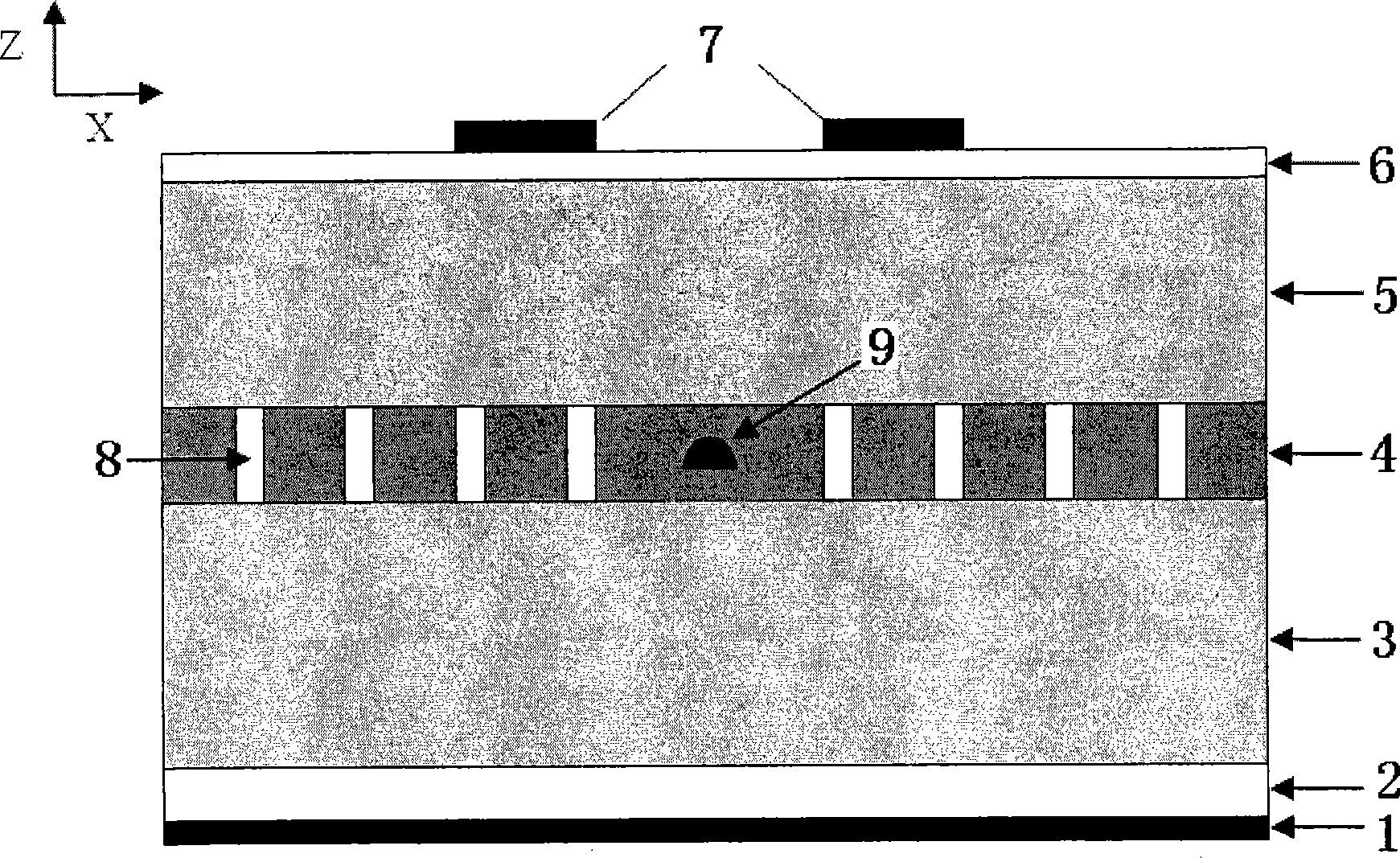
[0031] Such as figure 1 as shown, figure 1 Provided for the present invention is a schematic diagram of a vertical cross-sectional structure of a single photon source that uses photonic crystal microcavity and wafer bonding technology to realize electrical injection. The single photon source consists of a lower electrode 1, an n-type substrate 2, and a lower DBR 3 from bottom to top. , photonic crystal microcavity 4, upper DBR5, p-type contact layer 6 and upper electrode 7. The photonic crystal microcavity 4 has air holes 8 and quantum dots 9 .

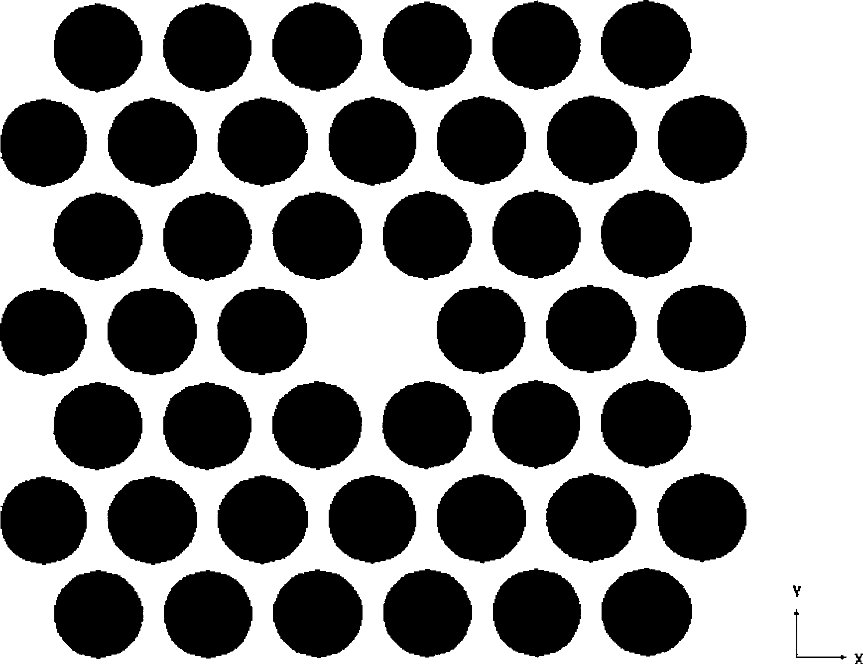
[0032] The photonic crystal microcavity is a semiconductor quantum dot photonic crystal microcavity, and adopts a two-dimensional photonic lattice air hole type defect cavity. ...


PUM


Abstract

The invention discloses a single-photon source, which realizes the electrical injection with the photonic crystal micro cavity and the wafer bonding technology. The single-photon source comprises a bottom electrode, an n-shaped substrate, a lower DBR, a photonic crystal micro cavity, an upper DBR, a p-shaped contact layer and a top electrode, which are arranged in sequence from bottom to top; wherein, the photonic crystal micro cavity of the single-photon source is provided with semiconductor quantum dots; the air hole type photonic crystal defect cavity with a two-dimensional photonic lattice is adopted; the single-photon source realizes the combination of the photonic crystal micro cavity and the upper DBR by adopting the wafer bonding technology; and the electrodes of the single-photon source are evaporated on the upper surface of the p-shaped contact layer and the lower surface of the n-shaped substrate of the upper DBR. The single-photon source not only realizes the electrical injection, but also improves the emission efficiency of the single-photon source.

Description

technical field [0001] The invention relates to the technical field of semiconductor optoelectronic devices, in particular to a single photon source for realizing electric injection by adopting photonic crystal microcavity and wafer bonding technology. Background technique [0002] As a new type of light source, single-photon source is a key part of quantum information technology, especially single-photon source with high efficiency, low probability of multi-photon generation and good quantum indistinguishability, in quantum key distribution, quantum computing and quantum The field of quantum information technology such as communication plays a pivotal role, and has become the focus of research in the field of quantum information technology in recent years. [0003] In the field of quantum information technology, the number of photons of the light source is required to be controllable, and it is hoped that each pulse of a single photon source will only generate one photon. ...

Claims


Application Information

Patent Timeline
IPC IPC(8): H01S5/00H01S5/10H01S5/34H01S5/042H01S5/06H01L33/00
Inventor 郑婉华刘安金任刚邢名欣渠宏伟陈良惠
Owner INST OF SEMICONDUCTORS - CHINESE ACAD OF SCI
Why Eureka
Try Eureka