Trans-impedance amplifier with low noise and high gain-bandwidth product
A technology of transimpedance amplifiers and amplifiers, applied in amplifiers with only semiconductor devices, amplifiers controlled by light, and improving amplifiers to reduce noise effects, etc. Open-loop characteristics and other issues to achieve the effect of reducing contribution, ensuring stability, and increasing signal bandwidth
- Summary
- Abstract
- Description
- Claims
- Application Information
AI Technical Summary
Problems solved by technology
Method used
Image
Examples
Embodiment 1
[0065] Figure 6 It is a schematic diagram (a) of the structure of the transimpedance amplifier TIA according to embodiment 1 of the present invention and an implementation of the schematic diagram (b) of its equivalent circuit. In the figure, PIN is a photoelectric converter that converts optical signals into current signals, A 1 is the main amplifier, A 2 are auxiliary amplifiers, and their open-loop gains are also denoted as A 1 、A 2 , and satisfy the condition:
[0066] A 1 >>1,A 2 1 ·A 2 =A ff >1;
[0067] Buffer is a buffer with a voltage gain of 1, which is not an indispensable part of this embodiment; R' in is the PIN shunt resistor R sh with the amplifier input resistor R in Equivalent resistance in parallel, C T is the total input capacitance of the TIA (including the PIN shunt capacitance C PIN , Amplifier input capacitance C in , amplifier input wiring capacitance and other parasitic capacitance C p etc.); R f is connection A 1 Output N to A 1 Neg...
Embodiment 2
[0104] Embodiment 2 of the present invention sees Figure 9 , PIN, A in the picture 1 、A 2 , Buffer, C T , R' in , R f 、C ff The definition of is the same as in Embodiment 1, C f is greater than R f The fixed capacitance of the parasitic capacitance can make the equivalent input capacitance of the TIA C ∑ will not be caused by R f The parasitic capacitance is unstable and affects the performance of the TIA. According to the analysis of embodiment 1, adjust A 2 The equivalent input capacitance of the TIA can be made to be approximately zero, so that a very high resistance value R f A wide signal bandwidth can also be obtained, and the noise voltage gain can be 0dB, making the TIA stable.
Embodiment 3
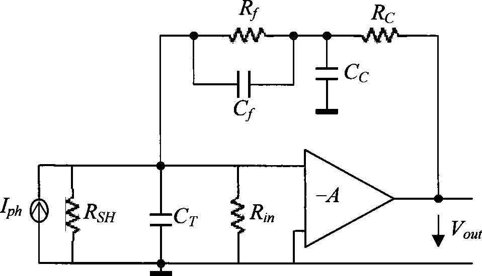
[0106] Embodiment 3 of the present invention sees Figure 10 As shown in the figure, PIN, A 1 、A 2 , Buffer, C T , R' in 、C ff The definition of is the same as that of embodiment 1, R f 、C f , R C 、C C Together make up A 1 The feedback network Z f , and satisfy the condition R f >>R c , C c >>C f , R f C f = R C C C . The difference from the implementations 1 and 2 is that the feedback network Z f The resulting equivalent input capacitance at the TIA input is C fin =C f C c / (C f +C c )≈C f , instead of (1+A in Embodiments 1 and 2 1 )C f , which allows a smaller capacitor value of C ff Compensate for the equivalent input capacitance of the TIA; the equivalent input resistance is R fin =(R f +R c ) / (1+A 1 )≈R f / (1+A 1 ), same as embodiment 1,2. Adjust A 2 It is also possible to make the equivalent input capacitance of the TIA approximately zero, thus using a very high resistance value R f A wide signal bandwidth can also be obtained, and the...
PUM
 Abstract
Description
Claims
Application Information


