High voltage device for drive chip of plasma flat-panel display

A flat-panel display and driver chip technology, applied in the direction of electric solid devices, semiconductor devices, electrical components, etc., can solve the problems of increased leakage current, increased device power consumption, etc., to achieve low conduction loss, improve integration density, and large saturation current. Effect

Inactive Publication Date: 2009-08-19
UNIV OF ELECTRONICS SCI & TECH OF CHINA
View PDF0 Cites 13 Cited by
  • Summary
  • Abstract
  • Description
  • Claims
  • Application Information

AI Technical Summary

Problems solved by technology

However, since HV-NMOS and HV-PMOS adopt silicon-based self-isolation technology, they have a large PN junction isolation area, and there is a parasitic PNP transistor consisting of p-type drift region 3, deep n well 2 and p substrate 1. possible
In addition, as the temperature rises, the leakage current of the reverse-biased PN junction will increase sharply, which will increase the power consumption of the device and easily lead to the HV-NMOS n-type drift region 4, p substrate 1, deep n well 2 and HV - The parasitic thyristor formed by the PMOS p-type drift region 3 is turned on

Method used


Image

  • High voltage device for drive chip of plasma flat-panel display
  • High voltage device for drive chip of plasma flat-panel display

Examples


Embodiment Construction

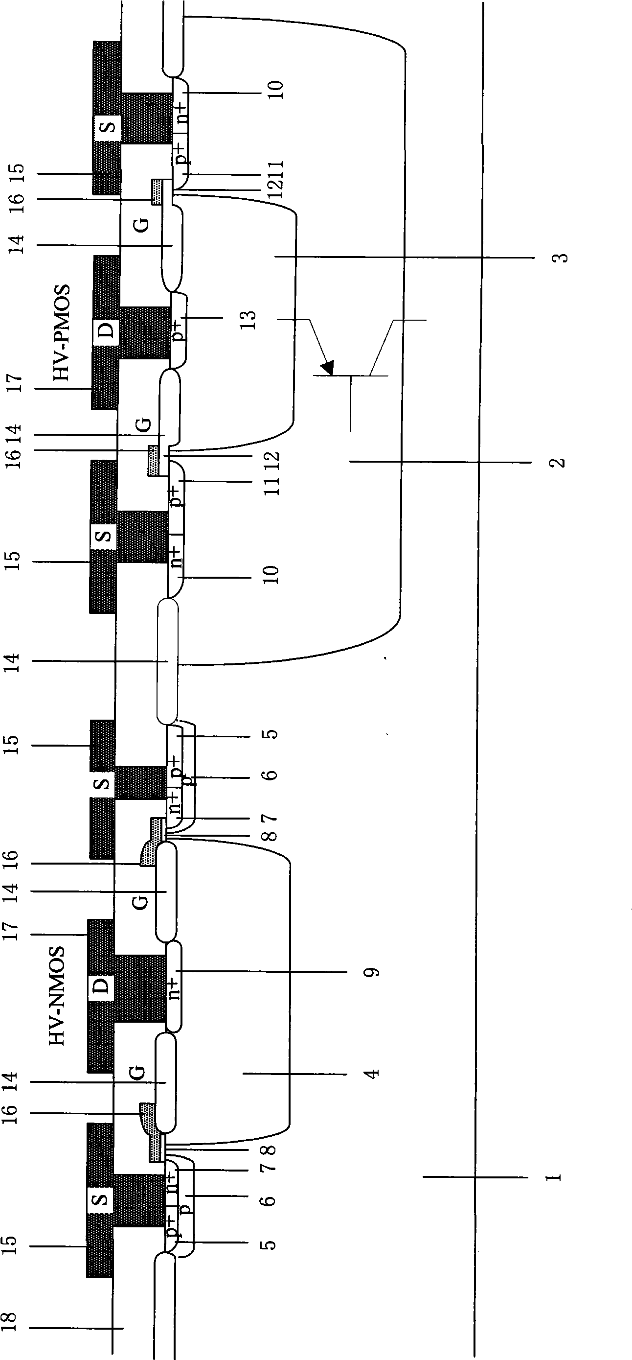
[0025] The invention realizes a 60V-300V high-voltage device based on the thick-layer SOI material, and has the characteristics of high speed, high integration and low power consumption. It satisfies the requirements of plasma flat panel display driver chips for high-voltage devices.

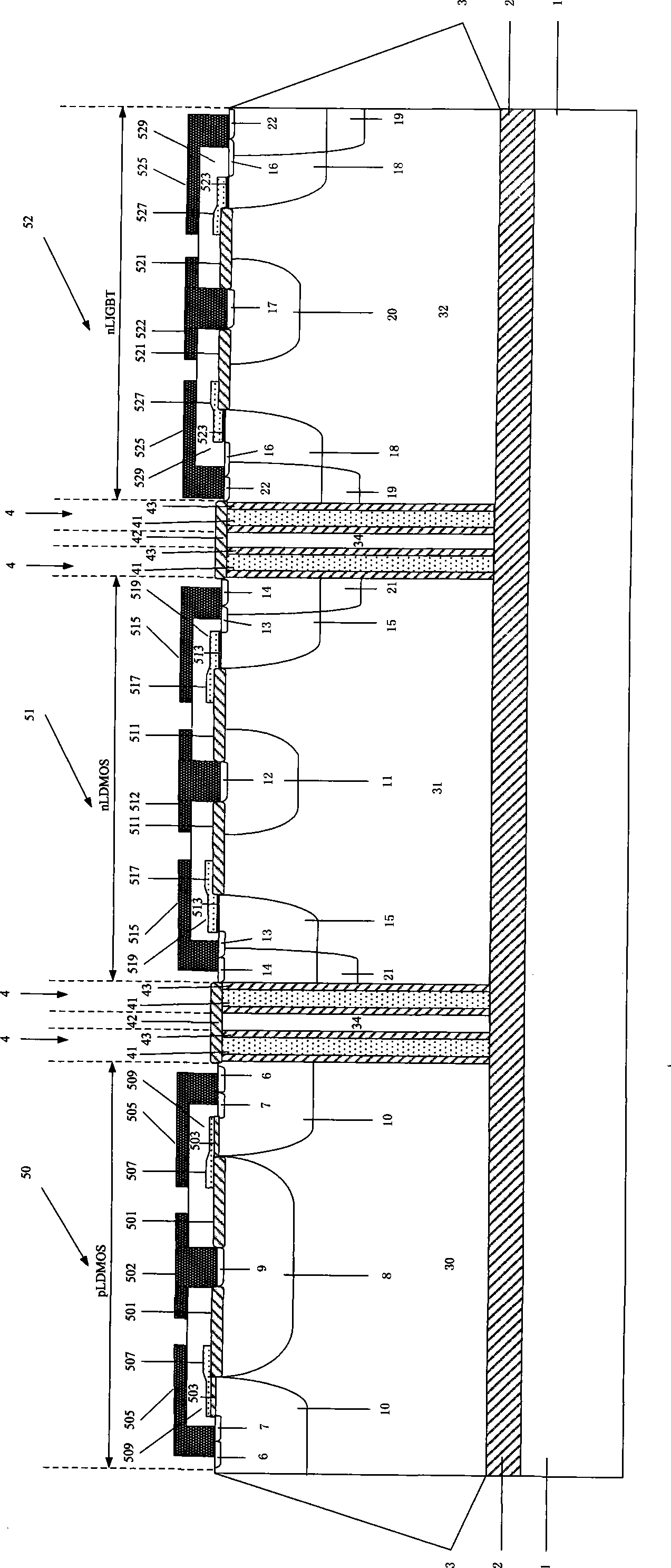
[0026] The high-voltage device for the plasma panel display driver chip of the present invention includes a high-voltage pLDMOS 50 , a high-voltage nLDMOS 51 and a high-voltage nLIGBT 52 . Wherein, 1 is a substrate, 2 is a buried oxide layer, 3 is an SOI layer, and 4 is a deep trench dielectric isolation region. The buried oxide layer 2 is located between the substrate 1 and the SOI layer 3, and the thickness of the SOI layer is 8-15 μm. The high-voltage pLDMOS 50, the high-voltage nLDMOS 51 and the high-voltage nLIGBT 52 are separated by the dielectric isolation region 4 to realize electrical isolation between high-voltage devices or high-voltage and low-voltage devices.

[0027] The high-vol...


PUM


Abstract

The invention provides a high-voltage device for a drive chip of a plasma flat-panel display, pertaining to the field of a semi-conductor power device. A high-voltage pLDMOS device, a high-voltage nLDMOS device and a high-voltage nLIGBT device are established on a substrate, an oxygen burying layer and an SOI layer and separated by deep-slot medium isolation areas. The oxygen burying layer and the deep-slot medium isolation areas positioned between the substrate and the SOI layer realize the full medium isolation of the device and low-voltage logic circuits. The thickness of the SOI layer is 8 micrometers and can meet the requirements of the device for high-voltage resistance. Compared with the thin SOI technology, the self-heating effect is relieved obviously and the nLIGBT device has low conduction resistance. The group of the high-voltage device for the drive chip of the plasma flat-panel display based on the thick SOI layer fully utilizes the characteristics of the SOI technology, such as low leak, small chip occupying area, high speed, high density of integration and low power consumption, thus meeting the development requirements of the large-sized plasma flat-panel display.

Description

technical field [0001] The invention belongs to the technical field of semiconductor power devices and is mainly applied to PDP (Plasma Display Panel) plasma flat panel display driver chips. Background technique [0002] Plasma display has become an excellent video display device and high-definition computer display because of its outstanding image effects and unique digital signal direct drive method. It is the development of large wall-mounted TVs, HDTV (High Definition Television) and large multimedia display screens. trend. Compared with LCD panels, plasma panels can complete the manufacture of products with the same production capacity with fewer processes, faster time, and lower equipment investment, and have wide viewing angles, long life, fast refresh speed, high light efficiency and brightness, and are easy to Make a large screen, wide operating temperature range and many other excellent features. With the development of plasma flat panel displays towards large si...

Claims


Application Information

Patent Timeline
Patent Type & Authority Applications(China)
IPC IPC(8): H01L27/12H01L29/78H01L29/06
Inventor 乔明杨帆廖红蒋苓利程鹏铭刘新新罗波张波
Owner UNIV OF ELECTRONICS SCI & TECH OF CHINA
Why Eureka
Try Eureka