Transparent conductive film glass
A technology of transparent conductive film and glass, which is applied in the direction of circuits, electrical components, electric solid devices, etc., can solve the problems of low light transmittance and resistivity in the visible spectrum region, reduce the working efficiency of devices, and large square resistance, so as to simplify the process flow , The effect that the gap between design and operability is low
- Summary
- Abstract
- Description
- Claims
- Application Information
AI Technical Summary
Problems solved by technology
Method used
Image
Examples
Embodiment 1
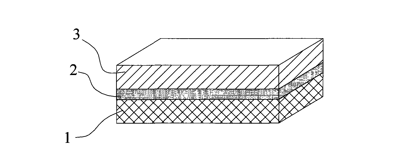
[0021] A glass with a transparent conductive film, comprising a base glass and a transparent conductive film, a low-resistance grid is arranged between the base glass and the transparent conductive film, and the transparent conductive film isolates the low-resistance grid from the external environment.
[0022] Among them, the bottom plate glass: ordinary optical glass is used.
[0023] Low-resistance grid: using medium-temperature aluminum paste as material, it is printed on the upper surface of the bottom glass at one time by screen printing method, and the low-resistance grid is printed into a mesh shape. The printing method is: use JG6080 screen printing machine, 300-mesh screen, and sinter at 450°C for half an hour after printing to make a low-resistance grid. The line width of the obtained low-resistance grid is 0.5mm.
[0024] Transparent conductive film: In 2 o 3 and SnO 2 Composite material, In 2 o 3 and SnO 2 The mass ratio is 1:1, and it is laid on the upper s...
Embodiment 2
[0027] A glass with a transparent conductive film, comprising a base glass and a transparent conductive film, a low-resistance grid is arranged between the base glass and the transparent conductive film, and the transparent conductive film isolates the low-resistance grid from the external environment.
[0028] Among them, the bottom plate glass: ordinary optical glass is used.
[0029] Low-resistance grid: Use low-temperature silver paste as the material, and use the screen printing method to print on the upper surface of the bottom glass at one time, and the low-resistance grid is printed in a linear shape. The printing method is: use JG6080 screen printing machine, 300-mesh screen, and sinter at 150°C for half an hour after printing to make a low-resistance grid. The line width of the obtained low-resistance grid is 0.5mm.
[0030] Transparent conductive film: SnO 2 : F composite film, SnO 2 The mass ratio with F is 5:1, and it is paved on the upper surface of the low-res...
Embodiment 3
[0033] A glass with a transparent conductive film, comprising a base glass and a transparent conductive film, a low-resistance grid is arranged between the base glass and the transparent conductive film, and the transparent conductive film isolates the low-resistance grid from the external environment.
[0034] Among them, the bottom plate glass: ordinary optical glass is used.
[0035] Low-resistance grid: low-temperature copper paste is used as the material, and the screen printing method is used to print on the upper surface of the bottom glass at one time, and the low-resistance grid is printed in a convoluted shape. Printing method: use JG6080 screen printing machine, 300-mesh screen, and sinter at 230°C for half an hour after printing to make a low-resistance grid. The line width of the obtained low-resistance grid is 0.5mm.
[0036] Transparent conductive film: In 2 o 3 :SnO 2 Composite film, In 2 o 3 with SnO 2 The mass ratio is 1:0.8, and the sol-gel (Sol-Gel) m...
PUM
 Abstract
Description
Claims
Application Information


