Double-substrate active layer structure with polysilicon layer and microcrystal silicon layer, method and device thereof

A polycrystalline silicon layer and microcrystalline silicon layer technology, which is applied in the direction of electrical components, electrical solid devices, circuits, etc., can solve the problems of inconsistent luminance of organic light-emitting diode displays, adverse effects of current density, and limited space for improvement, etc.

Active Publication Date: 2009-09-02
INNOLUX CORP
View PDF0 Cites 12 Cited by
  • Summary
  • Abstract
  • Description
  • Claims
  • Application Information

AI Technical Summary

Problems solved by technology

Since the above-mentioned laser annealing manufacturing process will affect the channel quality of the subsequent fabricated thin film transistors, it will have an adverse effect on the current density passing through each organic light emitting diode unit, resulting in inconsistent luminance of the organic light ...

Method used


Image

  • Double-substrate active layer structure with polysilicon layer and microcrystal silicon layer, method and device thereof
  • Double-substrate active layer structure with polysilicon layer and microcrystal silicon layer, method and device thereof

Examples


Embodiment Construction

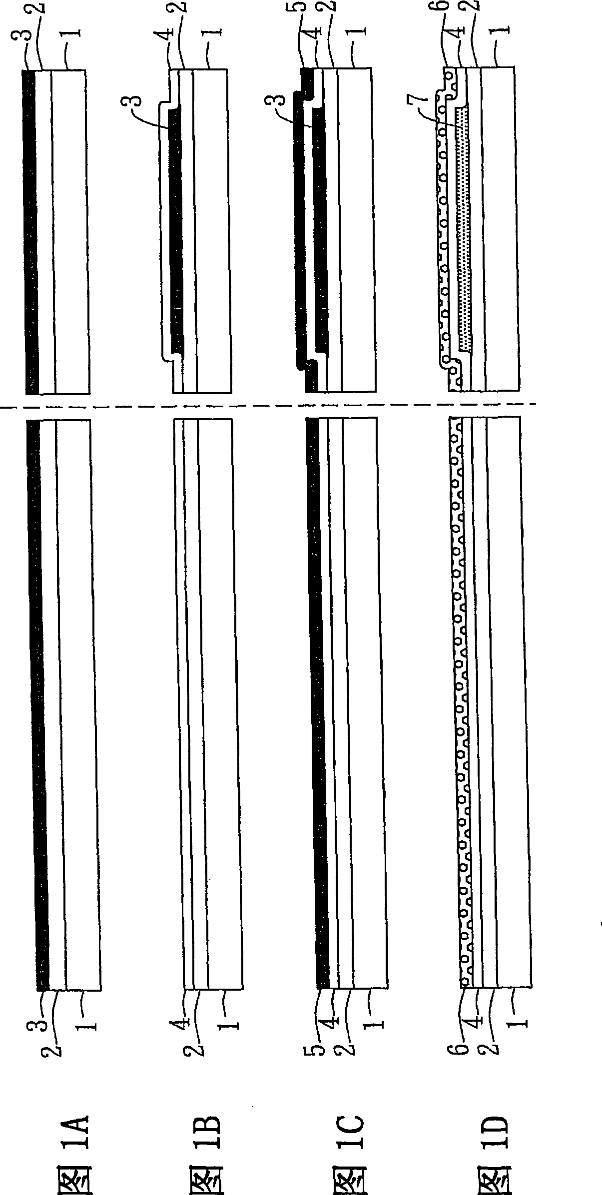
[0029] Refer to Figure 1A to Figure 1D It is a structural cross-sectional schematic diagram corresponding to each step of the manufacturing method of the dual-substrate active layer structure with a polysilicon layer and a microcrystalline silicon layer according to the present invention. With reference to Fig. 1A, the manufacturing method of the dual-substrate active layer structure with polysilicon layer and microcrystalline silicon layer of the present invention first provides a substrate 1, for example glass substrate or other semiconductor substrates, and the right side area of ​​a surface of described substrate 1 defines A display area and its left area define a driving circuit area. A buffer layer 2 is formed above the substrate 1 . Then a first amorphous silicon layer 3 is formed above the buffer layer 2 . Referring to FIG. 1B, the first amorphous silicon layer 3 is pattern etched to form a first active layer in the display area above the substrate 1, the first acti...


PUM

PropertyMeasurementUnit
Grain sizeaaaaaaaaaa

Abstract

The invention relates to a double-substrate active layer structure with a polysilicon layer and a microcrystal silicon layer, a method and a device thereof. The double-substrate active layer structure with the polysilicon layer and the microcrystal silicon layer comprises a base plate; the microcrystal silicon layer which is formed in a display area above the base plate and used as the active layer of a plurality of thin film transistors in the display area; and the polysilicon layer which is formed in a driving circuit area above the base plate and used as the active layer of a plurality of thin film transistors in the driving circuit area, wherein the grain size of the microcrystal silicon layer is less than that of the polysilicon layer. The light-emitting uniformity of an organic light-emitting diode can be improved by applying the invention.

Description

technical field [0001] The present invention relates to a thin film transistor display and its manufacturing method; more particularly, the present invention relates to a double substrate active layer structure with a polysilicon layer and a microcrystalline silicon layer and a thin film transistor display with the above structure and its manufacture method. Background technique [0002] The traditional manufacturing method of organic light-emitting diode displays is to form a buffer layer on the substrate before depositing the active layer of amorphous silicon, so that the laser annealing process (excimer laseranneal) is performed to crystallize the active layer of amorphous silicon When forming the active layer of polysilicon, it can isolate the impurities of the glass substrate from diffusing to the active layer due to the laser manufacturing process. However, when long-wavelength laser (wavelength greater than 400nm) is used in the laser annealing manufacturing process,...

Claims


Application Information

Patent Timeline
IPC IPC(8): H01L27/02H01L27/04H01L27/12H01L27/32H01L21/77H01L21/82H01L21/822H01L21/84H01L21/20
Inventor 刘侑宗李淂裕
Owner INNOLUX CORP
Why Eureka
Try Eureka