Photoelectric substrates

A technology for optoelectronic substrates and light guide plates, which is applied to optical waveguide light guides, coupling of optical waveguides, printed circuit components, etc. The effect of reducing production cost, increasing optical coupling efficiency and reducing transmission loss

Active Publication Date: 2008-05-14
IND TECH RES INST
View PDF1 Cites 5 Cited by
  • Summary
  • Abstract
  • Description
  • Claims
  • Application Information

AI Technical Summary

Problems solved by technology

However, because the bonding process of the circuit board and the light guide layer adopts the pressing process, which is a high-temperature and high-pressure process, and the optical waveguide is made of polymer materials, it is easy to deform under high temperature and high pressure, and the transition temperature of the optical waveguide It is only about 180°C. During the high-temperature and high-pressure process of the pressure plate, the optical path of the entire optical waveguide will be shifted. Even if it is returned to normal temperature and pressure, it still cannot return to the proper coupling efficiency, resulting in a large loss of optical signals.
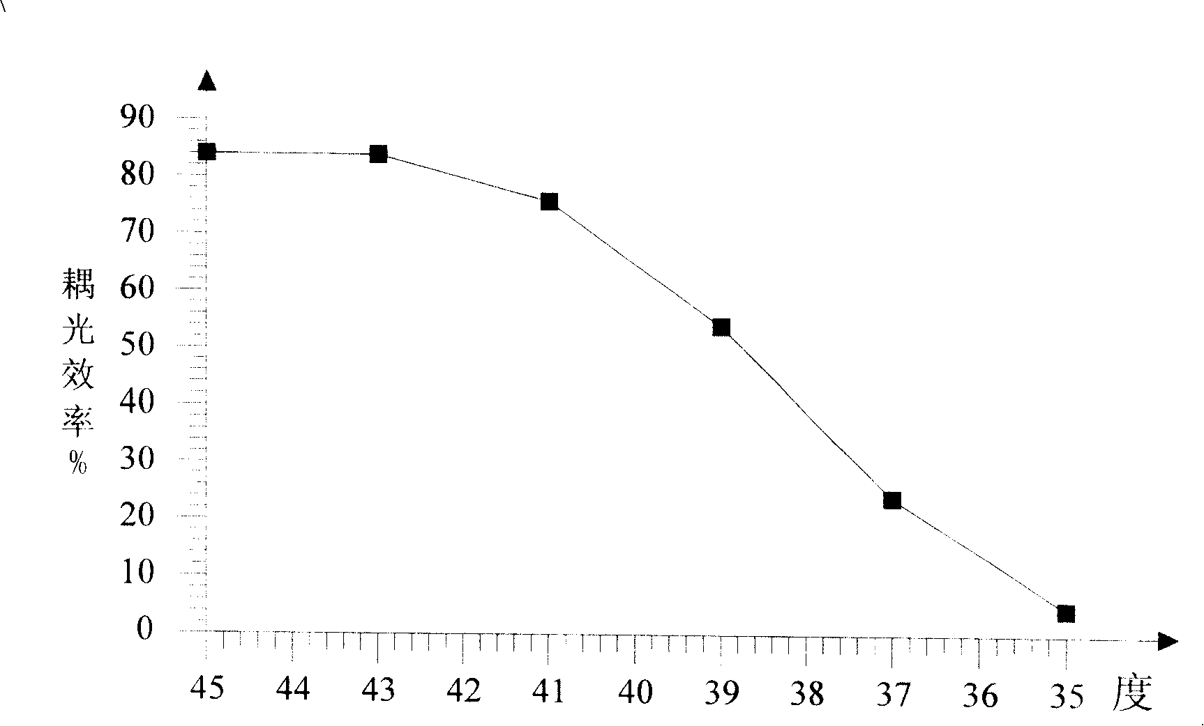
refer to image 3 , image 3 It is the curve graph of the mirror surface angle and light coupling efficiency of the optical waveguide of the prior art, such as image 3 As shown, in the press plate process, when the reflective mirror surface of the optical waveguide is deformed from 45° to 38°, the light coupling efficiency will drop from 83% to 39%

Method used


Image

  • Photoelectric substrates
  • Photoelectric substrates
  • Photoelectric substrates

Examples


Embodiment Construction

[0033] refer to Figure 4 , Figure 4 It is a schematic diagram of the first embodiment of the light guide plate 100 of the optoelectronic substrate of the present invention. Such as Figure 4 As shown, the light guide plate 100 of the first embodiment of the present invention includes a metal substrate 150, a glass fiber layer 130 formed on the metal substrate 150, a light guide layer 120 formed on the glass fiber layer 130, and a metal support The structure 152 is formed around the light guide layer 120 and on the glass fiber layer 130 .

[0034] The light guide layer 120 is composed of a waveguide and a cover layer 112 . In this embodiment, the optical waveguide is a multi-channel optical waveguide, which includes a plurality of cores (Cores) 110 embedded in the cladding layer 112 so that the cladding layer 112 can completely cover the cores 110 . Since the refractive index of the material selected for the cladding layer 112 is lower than that of the fiber core 110 , wh...


PUM


Abstract

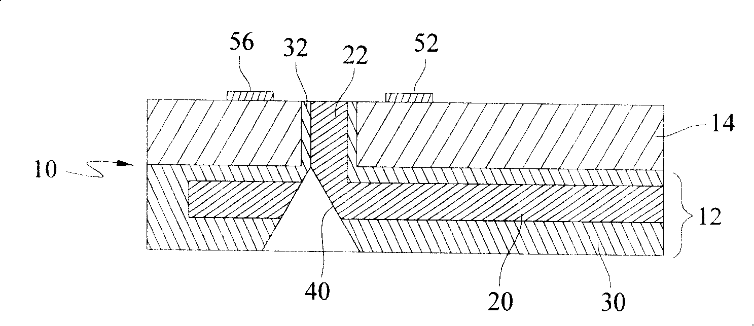
The invention discloses a photoelectric baseboard which comprises an electricity guide board and a light guide board. The light guide board comprises a first metal baseboard; a light guiding layer which is formed on the first metal baseboard and consists of a light-wave guide and a covering layer wrapping the light-wave guide; and a metal supporting structure which is formed on the surrounding of the light guiding layer. When the electricity guide board is jointed with the light guide board as a pressing board technique, the metal supporting structure can absorb the press being applied by the photoelectric baseboard. The invention combines the light-wave guide and a printing circuit board technique flow so as to lead the light-wave guide to become one layer in the printing circuit board and lead the light-wave guide to transmit light signals, and the invention utilizes the brass as the light guiding layer so as to increase the rigidity of the whole photoelectricity baseboard, prevent the distortion or damage caused by the high temperature and high pressure domino effects to the light-wave guide self during the board pressing technique, can form much better reflection surface, increase light-coupling efficiency and reduce the transmitting lost of the common light-wave guide and the light disturbing phenomena among multi-channel light-wave guide.

Description

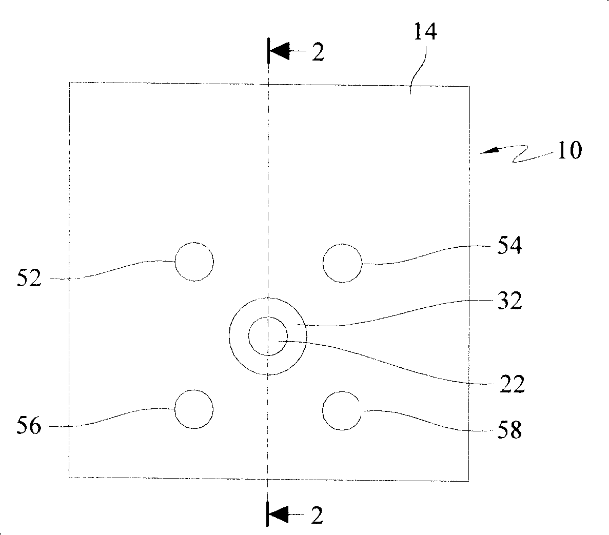
technical field [0001] The invention relates to a photoelectric substrate, in particular to a photoelectric substrate with an optical waveguide support structure. Background technique [0002] With the growth of the Internet (Internet), people's demand for network bandwidth is increasing day by day, and the optical fiber network is becoming more and more large-capacity, multi-variable, high-reliable, and economically effective. The development of optical communication, from the backbone network, metropolitan network, access network, and storage network, has been fully fiber-based, and optical networking (Optical Networking) has been realized step by step, and fiber-to-the-home has gradually formed. The bandwidth bottleneck will fall on the so-called "last meter". The last meter includes the following three areas: host-to-host (Rack to Rack), board-to-board (Board to Board), and chip-to-chip (Chip to Chip). Chip). [0003] At present, the short-distance interconnection tech...

Claims


Application Information

Patent Timeline
Patent Type & Authority Applications(China)
IPC IPC(8): G02B6/12G02B6/42H05K1/02
Inventor 吴承勋邱显桓李欣哲陈颖志
Owner IND TECH RES INST
Why Eureka
Try Eureka