Two-way low-voltage punch-through transient voltage suppression diode and manufacturing method thereof
A technology of transient voltage suppression and manufacturing method, which is applied in semiconductor/solid-state device manufacturing, circuits, electrical components, etc., can solve problems such as increased cost, and achieve the effects of low leakage current, excellent clamping characteristics, and low capacitance
- Summary
- Abstract
- Description
- Claims
- Application Information
AI Technical Summary
Problems solved by technology
Method used
Image
Examples
Embodiment 1
[0085] See Figure 3.1~3.6 As shown, in order to realize the structure diagram of the manufacturing process of the bidirectional low-voltage punch-through transient voltage suppression diode of the present invention, it specifically includes the following steps:
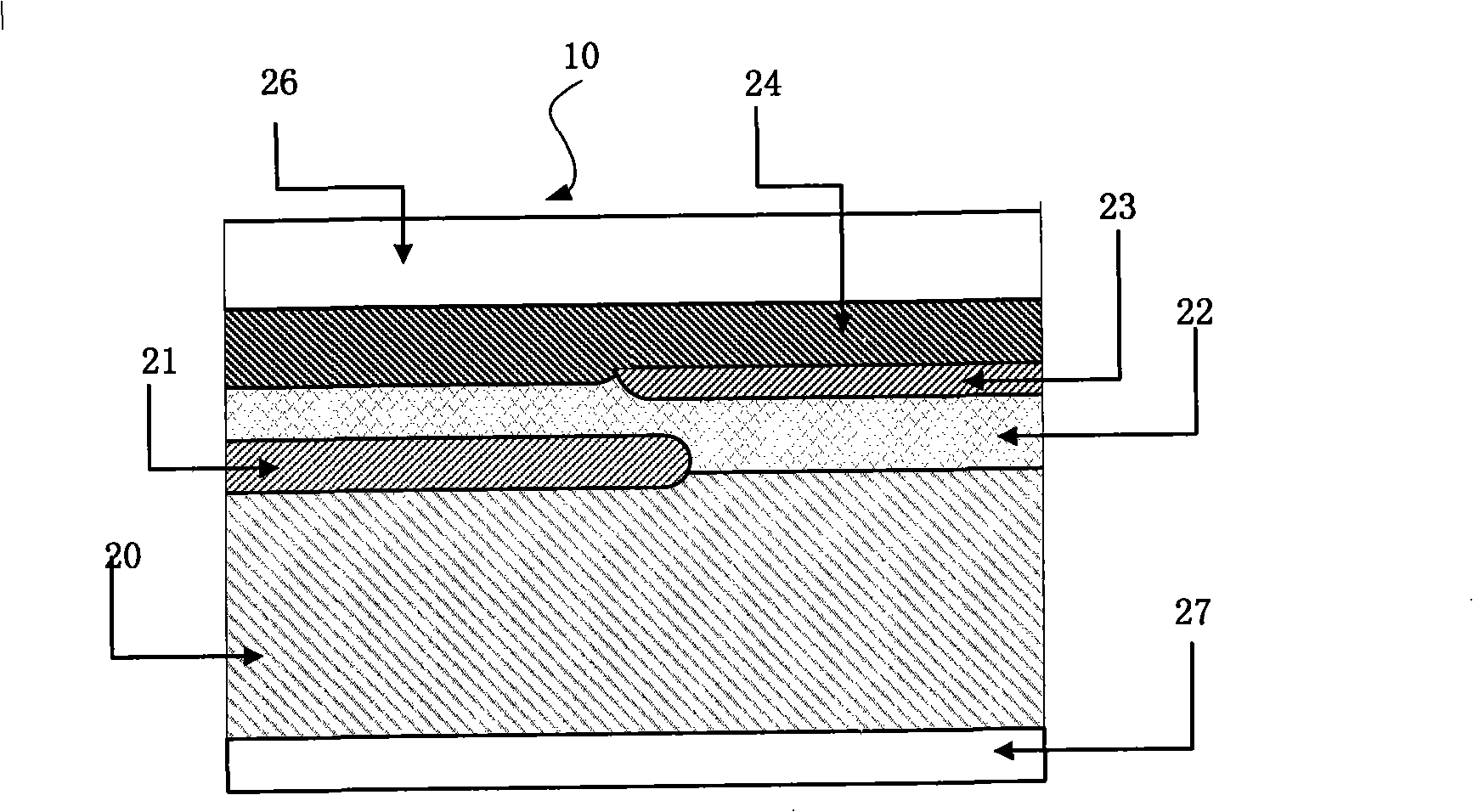
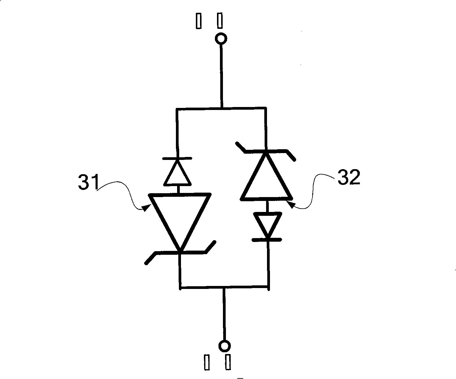
[0086] The first step: such as Figure 3.1 , The p+ buried layer 21 is formed by boron implantation and annealing in half of the n+ substrate 20. The p+ buried layer 21 laterally covers half of the n+ substrate 20. This p-type buried layer serves as the heavily doped base region of the reverse punch through diode. The n-type substrate serves as the emitter area of the reverse protection low-voltage punch-through diode 31 and the collector area of the forward protection low-voltage punch-through diode 32;
[0087] The second step: such as Figure 3.2 , Grow a lightly doped p- epitaxial layer 22 on the n+ substrate 20 with the p+ buried layer 21, half of the p- epitaxial layer 22 is on the n+ substrate 20, and the othe...
Embodiment 2
[0093] See Figure 4.1~4.7 As shown, in order to realize the structure diagram of the manufacturing process of the bidirectional low-voltage punch-through transient voltage suppression diode of the present invention, it specifically includes the following steps:
[0094] The first step: such as Figure 4.1 , The p+ buried layer 21 is formed by boron implantation and annealing in half of the n+ substrate 20. The p+ buried layer 21 laterally covers half of the n+ substrate 20. This p-type buried layer serves as the heavily doped base region of the reverse punch through diode. The n-type substrate serves as the emitter area of the reverse protection low-voltage punch-through diode 31 and the collector area of the forward protection low-voltage punch-through diode 32;
[0095] The second step: such as Figure 4.2 , Grow a lightly doped p- epitaxial layer 22 on the n+ substrate 20 with the p+ buried layer 21, half of the p- epitaxial layer 22 is on the n+ substrate 20, and the othe...
Embodiment 3
[0102] See Figure 5.1~5.6 As shown, in order to realize the structure diagram of the manufacturing process of the bidirectional low-voltage punch-through transient voltage suppression diode of the present invention, it specifically includes the following steps:
[0103] The first step: such as Figure 5.1 , The p+ buried layer 21 is formed by boron implantation and annealing in half of the n+ substrate 20. The p+ buried layer 21 laterally covers half of the n+ substrate 20. This p-type buried layer serves as the heavily doped base region of the reverse punch through diode. The n-type substrate serves as the emitter area of the reverse protection low-voltage punch-through diode 31 and the collector area of the forward protection low-voltage punch-through diode 32;
[0104] The second step: such as Figure 5.2 , Grow a lightly doped p- epitaxial layer 22 on the n+ substrate 20 with the p+ buried layer 21, half of the p- epitaxial layer 22 is on the n+ substrate 20, and the other...
PUM
 Abstract
Description
Claims
Application Information


