

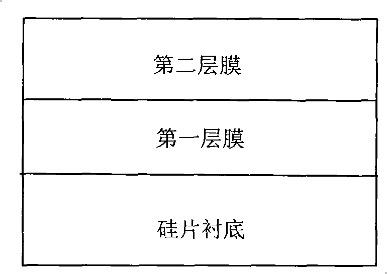
Anti-reflecting film applied to metallurgical silicon solar cell and preparation method thereof
A technology for solar cells and anti-reflection films, which is applied to the field of anti-reflection films on the surface of solar cells and their preparation, can solve the problem that a single-layer anti-reflection film is difficult to achieve an anti-reflection effect, etc., and achieves the advantages of improving photoelectric conversion efficiency and reducing reflection. Effect
- Summary
- Abstract
- Description
- Claims
- Application Information
AI Technical Summary
Problems solved by technology
Method used
Image

Examples
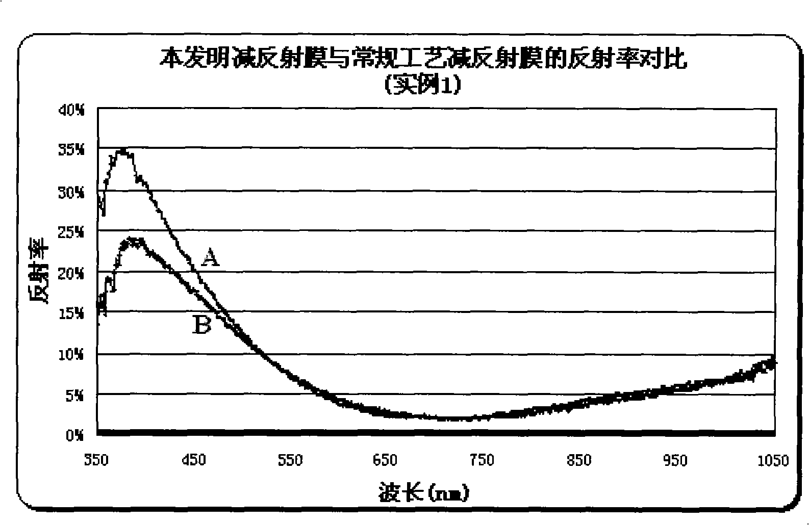
Embodiment 1
[0021] A group of silicon wafers (200 pieces) after the four steps of conventional silicon wafer cleaning, texturing, diffusion preparation of PN junction, etching and removal of PN junction around the silicon wafer, and cleaning and removal of phosphosilicate glass were processed as follows:
[0022] 1. Heating at 350°C for 28s; 2. Using PECVD equipment, the first-stage coating is carried out in a reaction atmosphere of silane and ammonia. The flow rate of silane is 900 sccm, the flow rate of ammonia gas is 310 sccm, and the process pressure is 3.0e -1 mbar, the microwave power is 3200W, and the transmission speed of the substrate is 100cm / min.; 3. Using PECVD equipment, the second-stage coating is carried out in the reaction atmosphere of silane and ammonia. The flow rate of silane is 1550 sccm, the flow rate of ammonia gas is 280 sccm, and the process pressure for 3.0e -1 mbar, the microwave power is 3200W, and the transmission speed of the silicon wafer carrier is 100cm / mi...
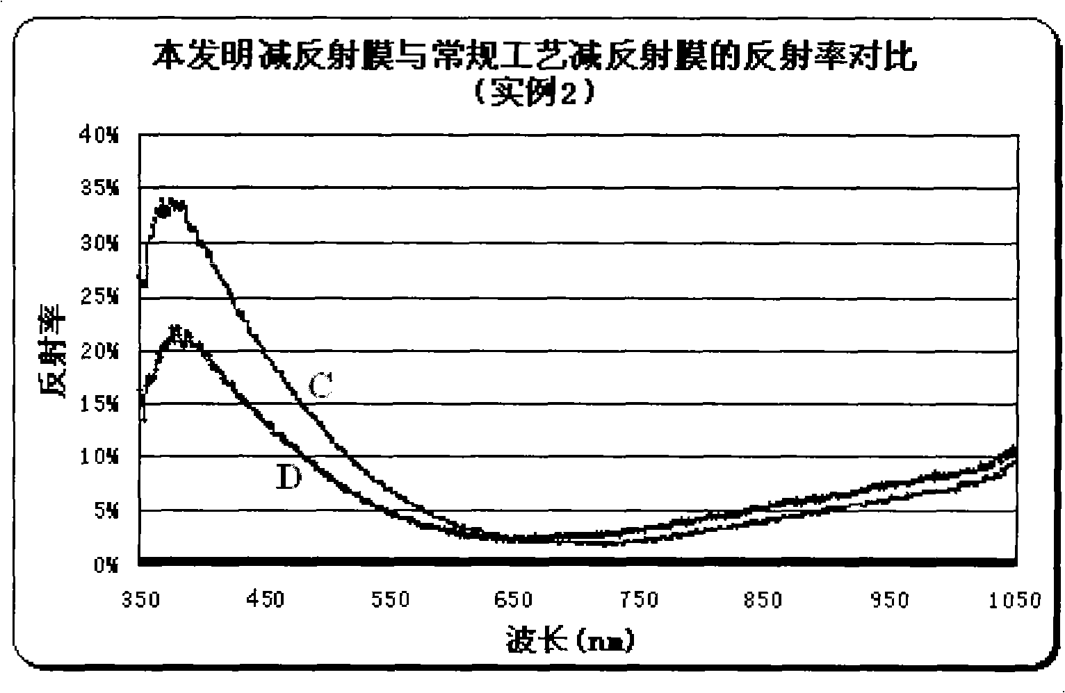
Embodiment 2
[0028] A group of silicon wafers (200 pieces) after the four steps of conventional silicon wafer cleaning, texturing, diffusion preparation of PN junction, etching and removal of PN junction around the silicon wafer, and cleaning and removal of phosphosilicate glass were processed as follows:
[0029] 1. Heating at 350°C for 30s; 2. Using PECVD equipment, in the first stage of coating in the reaction atmosphere of silane and ammonia, the flow rate of silane is 880sccm, the flow rate of ammonia gas is 305sccm, and the process pressure is 3.05e -1 , the microwave power is 3200W, and the transmission speed of the silicon wafer carrier plate is 105cm / min.; 3. Using PECVD equipment, the second-stage coating is carried out in the reaction atmosphere of silane and ammonia gas, the flow rate of silane is 1500 sccm, and the flow rate of ammonia gas is 270sccm, process pressure is 3.1e -1 , the microwave power is 3200W, and the transmission speed of the silicon wafer carrier is 105cm / mi...
Embodiment 3
[0039] A group of silicon wafers (200 pieces) after the four steps of conventional silicon wafer cleaning, texturing, diffusion preparation of PN junction, etching and removal of PN junction around the silicon wafer, and cleaning and removal of phosphosilicate glass were processed as follows:
[0040] 1. Heating at 350°C for 26s; 2. Using PECVD equipment, in the first stage of coating in the reaction atmosphere of silane and ammonia, the flow rate of silane is 850 sccm, the flow rate of ammonia gas is 300 sccm, and the process pressure is 3.0e -1 mbar, the microwave power is 3250W, and the transmission speed of the substrate is 103cm / min.; 3. Using PECVD equipment, the second-stage coating is carried out in the reaction atmosphere of silane and ammonia. for 3.0e -1 mbar, the microwave power is 3250W, and the transmission speed of the silicon wafer carrier is 103cm / min.
[0041] The two coating stages are completed continuously in the same process chamber. Finally, an anti-re...
PUM
| Property | Measurement | Unit |
|---|---|---|
| Thickness | aaaaa | aaaaa |
| Thickness | aaaaa | aaaaa |
| Film thickness | aaaaa | aaaaa |
Abstract
Description
Claims
Application Information