Thin film transistor

A thin film transistor and channel layer technology, applied in transistors, semiconductor devices, electrical components, etc., can solve problems such as large drain currents

Inactive Publication Date: 2009-09-23
CHUNGHWA PICTURE TUBES LTD
View PDF0 Cites 11 Cited by
  • Summary
  • Abstract
  • Description
  • Claims
  • Application Information

AI Technical Summary

Problems solved by technology

In addition, thin film transistor switching elements us

Method used


Image

  • Thin film transistor
  • Thin film transistor
  • Thin film transistor

Examples


no. 1 example

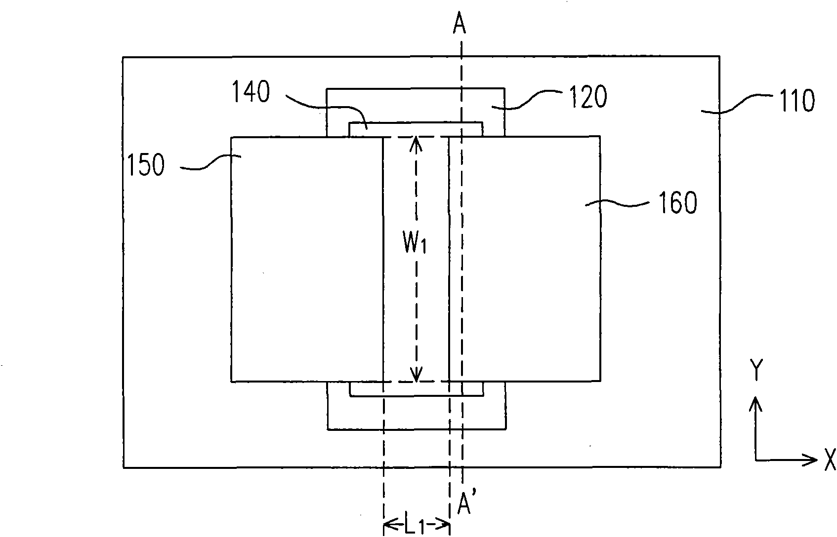
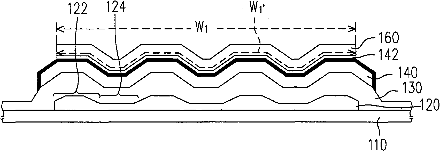
[0045] Figure 1A It is a schematic diagram of a thin film transistor according to an embodiment of the present invention. Figure 1B yes Figure 1A Sectional view of the structure along section line A-A'. in the text, Figure 1A The Y direction is the direction extending along the channel width W1, which is defined as the longitudinal direction, and the X direction is the direction extending along the channel length L1, which is defined as the lateral direction.

[0046] Please also refer to Figure 1A and Figure 1B . The TFT includes a gate 120 , a gate insulating layer 130 , a channel layer 140 , a source 150 and a drain 160 . Wherein, the gate 120 is disposed on a substrate 110 . The substrate 110 may be a transparent substrate 110 such as glass or quartz. The gate 120 can be fabricated by depositing a metal material on the substrate 110 by, for example, physical vapor deposition (PVD), and then patterning the metal material through a photomask process. The above-men...

no. 2 example

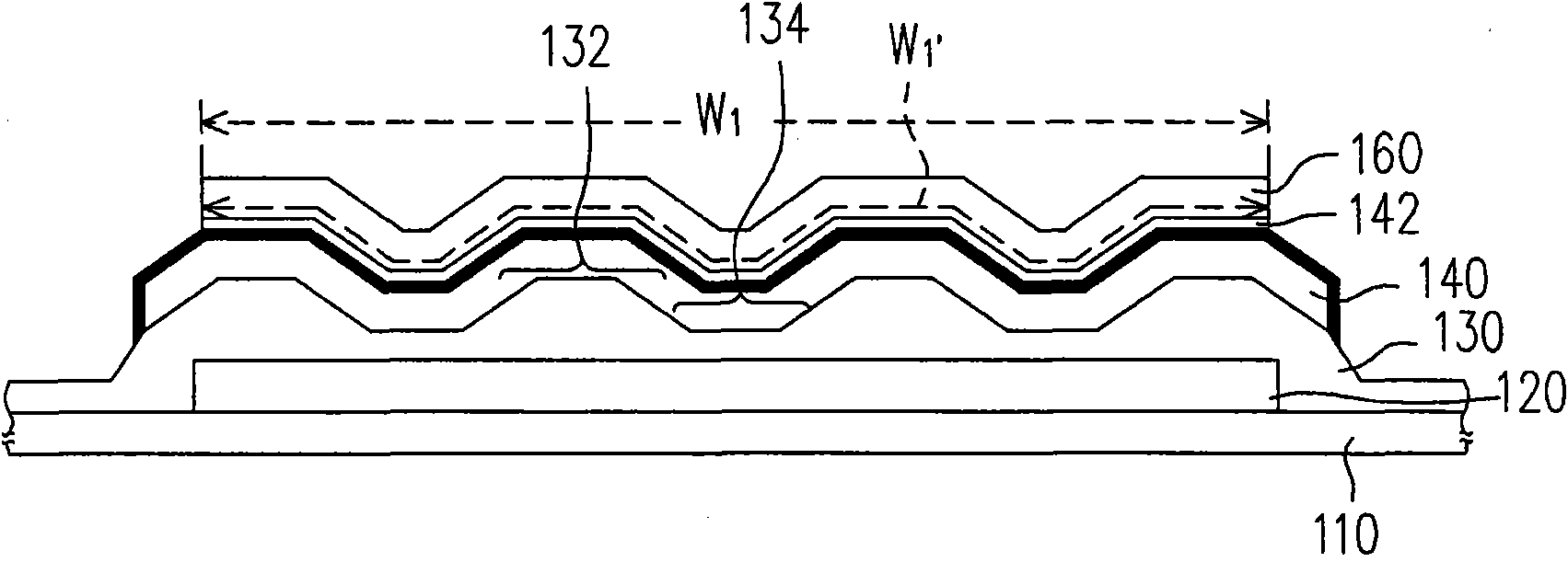
[0051] Figure 2A It is a schematic diagram of a thin film transistor according to another embodiment of the present invention, Figure 2B for Figure 2A Sectional view of the structure along section line B-B'. Please also refer to Figure 2A and Figure 2B , the thin film transistor includes a gate 120 , a gate insulating layer 130 , a channel layer 140 , a source 250 and a drain 260 . The gate 120 is disposed on a substrate 110 , and the gate insulating layer 130 covers the gate 120 . The substrate 110 may be a transparent substrate 110 such as glass or quartz. The gate 120 can be fabricated by depositing a metal material on the substrate 110 by, for example, physical vapor deposition (PVD), and then patterning the metal material through a photomask process. The above-mentioned metal materials can be selected from low-resistance materials such as aluminum, gold, copper, molybdenum, chromium, titanium, aluminum alloy or molybdenum alloy.

[0052] In addition, the gate ...


PUM


Abstract

The invention provides a thin film transistor, which comprises a grid, a grid insulating layer, a channel layer, a source electrode and a drain electrode, wherein the grid is arranged on a substrate; the grid insulating layer is covered on the grid; the channel layer is arranged on the grid insulating layer above the grid; the longitudinal section of the channel layer can be of a wave shape; and the source electrode and the drain electrode are arranged on the channel layer; in addition, the longitudinal section of the channel layer can be flat in surface, and the source electrode and the drain electrode at two sides covered on the channel layer are in nonlinear line list structures.

Description

technical field [0001] The present invention relates to a thin film transistor, and in particular to a thin film transistor with better output characteristics. Background technique [0002] In recent years, with the maturity of optoelectronic technology and semiconductor manufacturing technology, flat panel displays (Flat Panel Displays) have flourished, and liquid crystal displays have gradually replaced them based on their advantages of low voltage operation, no radiation scattering, light weight and small size. Traditional cathode ray tube displays have become the mainstream of display products in recent years. [0003] A general liquid crystal display is mainly composed of a thin film transistor array substrate, a color filter substrate and a liquid crystal layer located between the two substrates, wherein the thin film transistor array substrate has a plurality of pixel units arranged in a matrix, and each pixel unit includes a The thin film transistor and a pixel elec...

Claims


Application Information

Patent Timeline
IPC IPC(8): H01L29/786H01L29/10H01L29/423H01L29/417
Inventor 张锡明
Owner CHUNGHWA PICTURE TUBES LTD
Why Eureka
Try Eureka