S waveband arborization left-handed material microstrip antenna
A technology of left-handed materials and microstrip antennas, applied in antennas, structural forms of radiation elements, electrical components, etc., can solve the problems of low gain, low radiation efficiency of ordinary microstrip antennas, and narrow frequency band, etc., and achieve the effect of simple process
- Summary
- Abstract
- Description
- Claims
- Application Information
AI Technical Summary
Problems solved by technology
Method used
Image
Examples
Embodiment 1
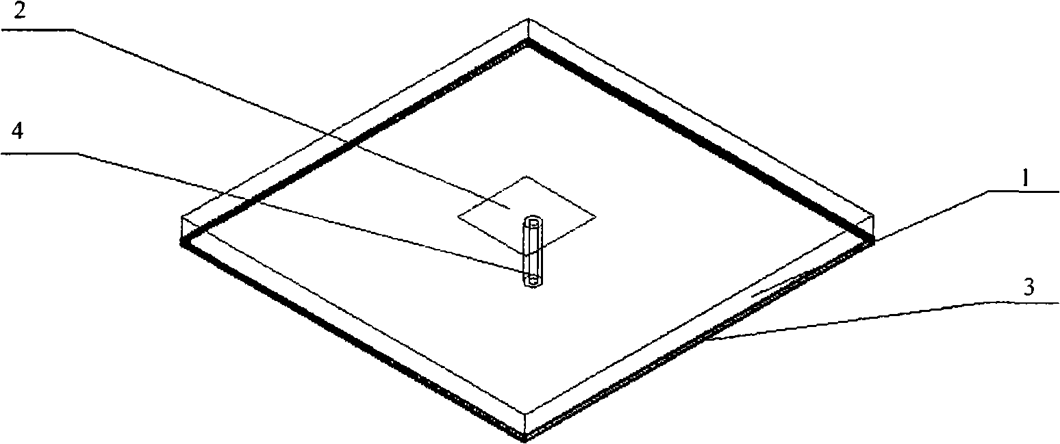
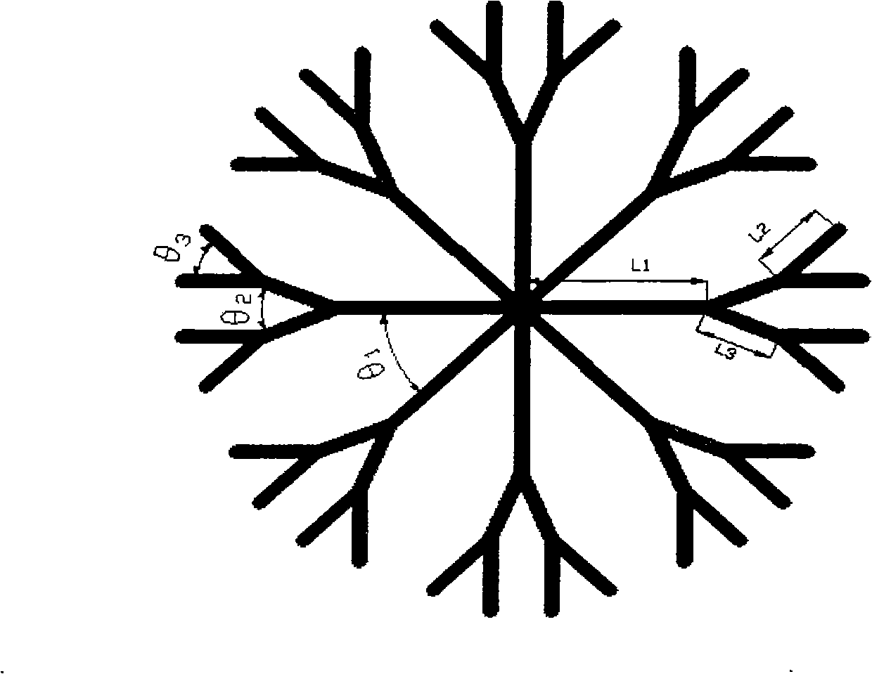
[0016] Using circuit board etching technology, a dendritic structure left-handed material microstrip antenna with a center operating frequency of 2.95GHz is produced, such as Figure 4 shown. A polytetrafluoroethylene material (ε=2.65) with an area of 160mm×160mm and a thickness of 1.5mm is selected as the dielectric substrate 1 of the antenna, and the size of the metal copper radiation patch 2 on one side of the dielectric substrate 1 is 37mm×30mm, and on the other side It is entirely made of metal copper, as the ground plate 3, using coaxial feed, and the SMA coaxial 4 connector connects the metal radiation plate 2 and the metal ground plate 3, and serves as the signal feed source of the antenna. The metal copper dendritic structure unit array 5 is etched periodically around the radiation patch. For the microstrip antenna with a working frequency of 2.95 GHz in this embodiment, the geometric dimension of the dendritic structure is: the length of the primary branch L 1 =8....
Embodiment 2
[0018] Using circuit board etching technology, a dendritic structure left-handed material microstrip antenna with a central operating frequency of 2.6GHz is produced, such as Figure 4 shown. The epoxy glass cloth material (ε=4.55) with an area of 180mm×180mm and a thickness of 0.8mm is selected as the dielectric substrate 1 of the antenna. The size of the metal copper radiation patch 2 on one side of the dielectric substrate 1 is 43mm×35mm, and the other side is completely It is made of metal copper, used as the ground plate 3, and coaxial feed is used, and the SMA coaxial 4 connector connects the metal radiation plate 2 and the metal ground plate 3, and serves as the signal feed source of the antenna. The metal copper dendritic structure element array 5 is etched periodically around the radiation patch. For the microstrip antenna with a working frequency of 2.6 GHz in this embodiment, the geometric dimension of the dendritic structure is: the primary branch length L 1 =8....
Embodiment 3
[0020] Using circuit board etching technology, a dendritic structure left-handed material microstrip antenna with a center operating frequency of 3.4GHz is produced, such as Figure 4 shown. A polyethylene material (ε=2.3) with an area of 140mm×140mm and a thickness of 1.0mm is selected as the dielectric substrate 1 of the antenna. The size of the metal copper radiation patch 2 on one side of the dielectric substrate 1 is 33mm×26mm, and the other side is completely Metal copper, as the ground plate 3, adopts coaxial feed, and the SMA coaxial 4 connector connects the metal radiation plate 2 and the metal ground plate 3, and serves as the signal feed source of the antenna. The metal copper dendritic structure element array 5 is etched periodically around the radiation patch. For the microstrip antenna with a working frequency of 3.4 GHz in this embodiment, the geometric dimension of the dendritic structure is: the primary branch length L 1 =7.1, the length of the secondary br...
PUM
| Property | Measurement | Unit |
|---|---|---|
| Lattice constant | aaaaa | aaaaa |
| Thickness | aaaaa | aaaaa |
| Thickness | aaaaa | aaaaa |
Abstract
Description
Claims
Application Information


