Built-in self-testing method of FPGA input/output module

An input and output module, built-in self-test technology, applied in the direction of measuring electricity, measuring devices, measuring electrical variables, etc., can solve the problems of difficult test implementation, complicated theoretical design, and time-consuming testing, so as to reduce the number of test configurations, The effect of simplifying retrieval methods and reducing testing costs

Active Publication Date: 2009-10-07
BEIJING MXTRONICS CORP +1
View PDF0 Cites 37 Cited by
  • Summary
  • Abstract
  • Description
  • Claims
  • Application Information

AI Technical Summary

Problems solved by technology

At present, foreign countries have conducted research on the testing of FPGA logic resources, and proposed a built-in self-test theory based on memory readback, but these theories are complex in design, and the test result readback and diagnosis

Method used


Image

  • Built-in self-testing method of FPGA input/output module
  • Built-in self-testing method of FPGA input/output module
  • Built-in self-testing method of FPGA input/output module

Examples


Embodiment Construction

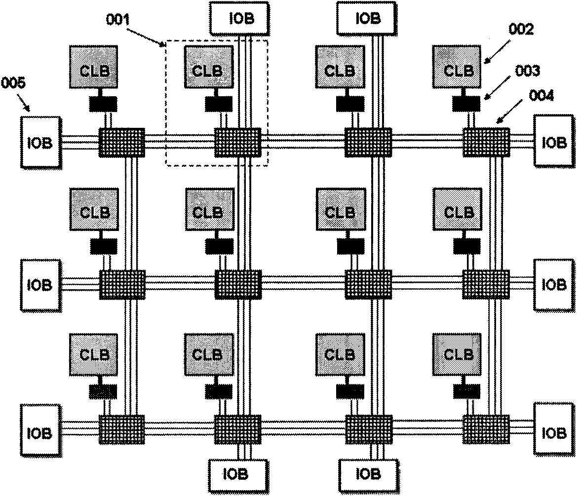
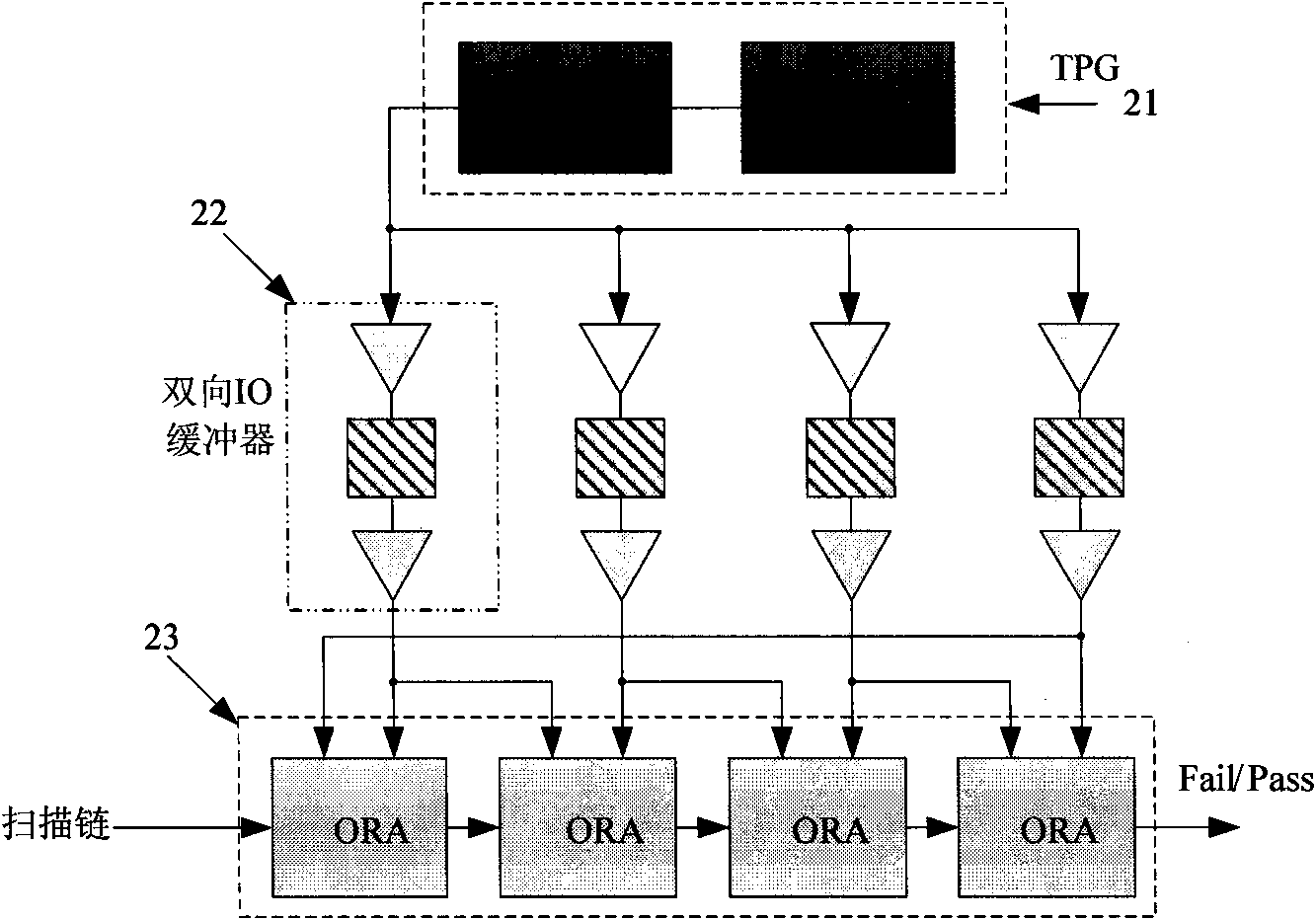
[0025] FPGA basic circuit structure such as figure 1 As shown, it is mainly composed of TITLE array 001 and input and output module 005. Programmable logic module 002 is a logic unit in one of TITLE array 001, and it realizes interconnection with surrounding programmable logic modules through IMUX003 and switch matrix 004 , users can flexibly implement various functions by configuring the programmable logic module 002. In traditional FPGA testing methods, it is often necessary to first ensure the correct function of the input and output modules before testing other modules. In the present invention, all input and output modules are configured as bidirectional IO buffers, such as figure 2 As shown, the internal resources of the IO buffer are tested through the optimized configuration, and the test results are output through the scan register chain. First part logic resources are configured into test vector generation circuit 21 and output response analysis circuit 23, all IO...


PUM


Abstract

The present invention provides a built-in self-testing method of FPGA input/output module. Firstly all input/output modules in FPGA are configured to that a bidirectional IO buffer is used as a circuit to be tested. The logical resource of middle part of FPGA device is configured to a test vector generating circuit. The logical resource surrounding the IO buffer is configured to an output response analysis circuit of scanning chain structure. In testing, the test vector generating circuit generates a pseudo-random exhaustive vector for exerting a test pattern for each circuit to be tested; after executing the test vector, actuating the operation of scanning chain of output response analysis circuit, outputting the built-in self-testing result which is configured this time by the input/output module in the control of test clock by the output response analysis circuit until when the test covers all resources in the input/output module. The method of the invention has the following advantages: simplified built-in self-testing result retrieval mode, reduced test configuration number of times, reduced test cost and increased test efficiency under the precondition of guaranteeing 100% test coverage rate.

Description

technical field [0001] The invention relates to a testing method of an FPGA chip, in particular to a built-in self-testing method of an FPGA input and output module based on a scan chain structure. Background technique [0002] FPGA testing takes advantage of its reprogrammable feature to cover all resources under test through multiple configurations. There are mainly two methods for its testing: external testing and built-in self-testing. During external testing, the FPGA device is configured as a corresponding testing circuit, and external equipment is used to apply test vectors and special equipment to analyze the output results. This testing method depends on packaging; and Compared with the external test, the vector application and response analysis of the built-in self-test method are completed internally, without the need for special test equipment and a large number of pins, which reduces the test cost and increases the test flexibility. [0003] The I / O module is t...

Claims


Application Information

Patent Timeline
IPC IPC(8): G01R31/3185G01R31/3187
Inventor 张志权文治平陈雷李学武储鹏张彦龙
Owner BEIJING MXTRONICS CORP
Why Eureka
Try Eureka