Double-stage switching system of photoetching machine wafer stage

A technology for exchanging systems and wafer stages, which is applied in the field of dual-stage exchanging systems for lithography machine wafer stages, can solve problems such as complex structure, high processing and assembly precision, achieve large air gap, reduce installation accuracy requirements, and avoid extreme The effect of high precision requirements

Active Publication Date: 2009-10-07
TSINGHUA UNIV +1
View PDF3 Cites 12 Cited by
  • Summary
  • Abstract
  • Description
  • Claims
  • Application Information

AI Technical Summary

Problems solved by technology

[0008] Aiming at the deficiencies and defects of the prior art, the purpose of the present invention is to provide a new double-swap exchange system for photolithography machines to overcome the complex structure and extremely high processing and processing requirements of the existing double-swap exchange system for silicon wafers. The disadvantages such as assembly accuracy make it have the advantages of simple structure, high space utilization and no collision between the upper linear guide rails of the dual-degree-of-freedom drive unit during exchange, thereby improving the exposure efficiency of the lithography machine

Method used


Image

  • Double-stage switching system of photoetching machine wafer stage
  • Double-stage switching system of photoetching machine wafer stage
  • Double-stage switching system of photoetching machine wafer stage

Examples


Embodiment Construction

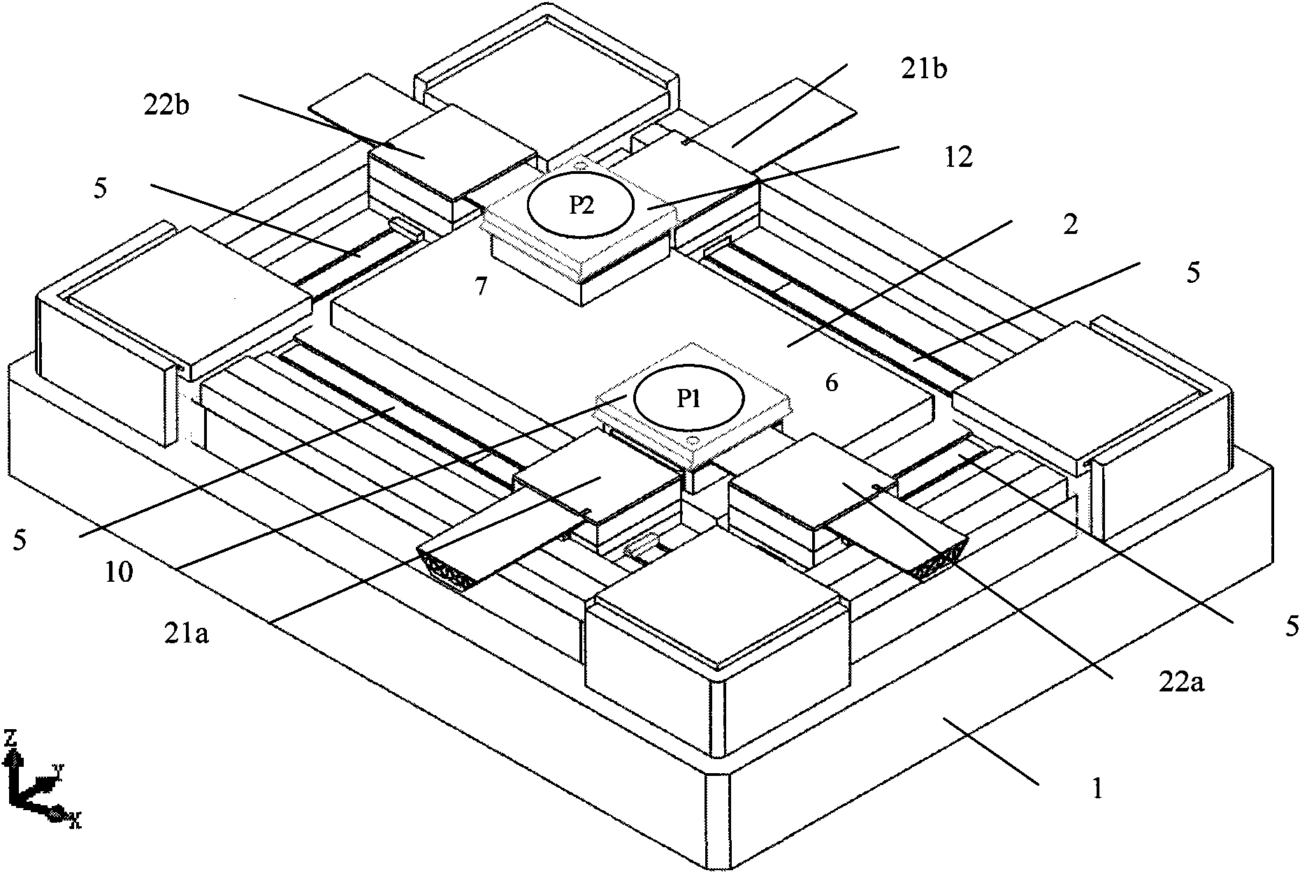
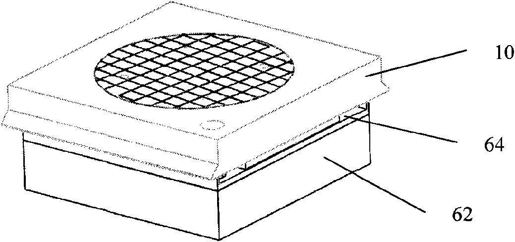
[0028] figure 2 It shows the structural schematic diagram of the dual wafer stage exchange system of the lithography machine. The system includes the base 1, the long side of the base is in the X direction, the short side is in the Y direction, and there is the first wafer stage running in the exposure station 6 10, the second wafer stage 12 running in the pre-processing station 7, and four dual-degree-of-freedom drive units arranged on the edge of the platform along the X-direction and Y-direction. The two silicon wafer stages are located in the space surrounded by four dual-degree-of-freedom drive units, and are suspended on the upper surface of the base stage through air bearings. The push rod of the first two-degree-of-freedom drive unit 21a in the X direction is fixed to the six-degree-of-freedom micro-motion table base 62 of the wafer stage, and the push rod of the first two-degree-of-freedom drive unit 22a in the Y direction is connected to the six-degree-of-freedom mi...


PUM


Abstract

The invention provides a double-stage switching system of photoetching machine wafer stage, wherein the system comprises a wafer stage operating on exposure station and a wafer stage operating on preprocess station, each wafer stage is bore by a six-freedom-degree microchecker, one wafer stage and one six-freedom-degree microchecker compose a wafer stage group, the two wafer stage groups is fixed on a rectangular base station. a group of double-freedom-degree driving units is fixed on each edge of the base station respectively, the two wafer stage groups suspends on surface of the base station by air-float bearings; the six-freedom-degree microchecker has upper and lower two layers, capable of implementing six-freedom-degree control, the double freedom degree driving units on edges of the base station is connected with the casing of the microchecker for driving the whole wafer stage group on a horizontal plane, the double-freedom-degree units on short edges of the microchecker are connected with the stator coil framework of the upper layer for driving the six-freedom-degree microcheckers moving on a horizontal plane of the upper layer stator coil. The invention avoids defects of high require process and assembly precision because of employing butt joint of guiding rails and need of butt joint auxiliary device increase, thereby greatly simplifying system structure.

Description

technical field [0001] The invention relates to a double-swap exchange system for silicon wafer tables of a lithography machine. The system is applied to a semiconductor lithography machine and belongs to the technical field of semiconductor manufacturing equipment. Background technique [0002] In the production process of integrated circuit chips, the exposure transfer (photolithography) of the design pattern of the chip on the photoresist on the surface of the silicon wafer is one of the most important processes. The equipment used in this process is called a photolithography machine (exposure machine). The resolution and exposure efficiency of the lithography machine greatly affect the characteristic line width (resolution) and productivity of the integrated circuit chip. As the key system of the lithography machine, the motion accuracy and work efficiency of the silicon wafer ultra-precision motion positioning system (hereinafter referred to as the wafer stage) largely...

Claims


Application Information

Patent Timeline
Patent Type & Authority Applications(China)
IPC IPC(8): G03F7/20
CPCG03F7/70758H01L21/682G03F7/70733
Inventor 朱煜张鸣汪劲松田丽徐登峰尹文生段广洪胡金春
Owner TSINGHUA UNIV
Why Eureka
Try Eureka