Chip of three-dimensional MEMS geophone and preparation method thereof

A geophone and chip technology, applied in seismic signal receivers, instruments, welding equipment, etc., can solve the problems of inconvenient detection of three-dimensional seismic signals, uneconomical and other problems, and achieve the effect of high resolution, high fidelity and large dynamic range

Inactive Publication Date: 2011-09-28
SOUTHWEST PETROLEUM UNIV
View PDF0 Cites 0 Cited by
  • Summary
  • Abstract
  • Description
  • Claims
  • Application Information

AI Technical Summary

Problems solved by technology

However, the current three-component digital sensor is a three-component digital sensor installed at right angles to three MEMS acceleration sensors. Responsiveness, etc. need to be further improved

Method used


Image

  • Chip of three-dimensional MEMS geophone and preparation method thereof
  • Chip of three-dimensional MEMS geophone and preparation method thereof
  • Chip of three-dimensional MEMS geophone and preparation method thereof

Examples


Embodiment 1

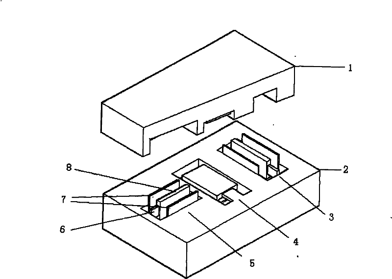
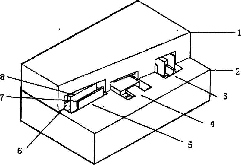
[0029] Such as figure 1 , 2 As shown, in two pieces of 20×20×0.5mm 2 Fabricate a three-dimensional MEMS geophone chip array on silicon wafers 1 and 2:

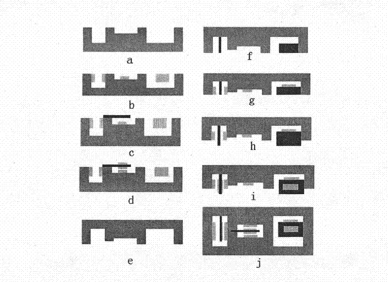
[0030] (1) Use a piece of 20×20×0.5mm 2 The silicon wafer is used as the substrate A2. After cleaning, three grooves are formed by photolithography. The three grooves are arranged at right angles and orthogonally. The depth of the grooves in the X and Z axis directions is 20-40 μm. The groove is 3μm deep, such as image 3 Shown in a; Sputter again to form a layer of 0.5 μm gold, and the wires and fixed electrodes 7 formed by stripping, such as image 3 as shown in b;

[0031] (2) By spin-coating polyimide 3 μm organic sacrificial layer for micromechanics, a cantilever beam model is formed on the sacrificial layer by photolithography, and a 2.5 μm thick silicon cantilever beam material is deposited by magnetron sputtering to remove the sacrificial material After layering, a cantilever beam 6 and a quality block 8 are form...

Embodiment 2

[0039] Such as figure 1 , 2 As shown, in two pieces of 20×20×0.5mm 2 Fabricate a three-dimensional MEMS geophone array on silicon wafers 1 and 2:

[0040] (1) Use a piece of 20×20×0.5mm 2 The silicon wafer is used as the substrate A2, and three grooves are formed by photolithography after cleaning, among which the depth of the grooves in the X and Z axis directions is 30 μm, and the depth of the grooves in the Y axis direction is 3 μm. image 3 Shown in a; Sputter again to form a layer of 0.5 μm gold, and the wires and fixed electrodes 7 formed by stripping, such as image 3 as shown in b;

[0041] (2) By spin-coating an organic sacrificial layer (polyimide) of 4 μm for micromechanics, a cantilever beam model is formed on the sacrificial layer by photolithography, and a silicon cantilever beam material with a thickness of 2.5 μm is deposited by magnetron sputtering, After removing the sacrificial layer, a cantilever beam 6 and a mass block 8 are formed, such as image 3 ...

Embodiment 3

[0049] Such as figure 1 , 2 As shown, in two pieces of 20×20×0.5mm 2 Fabricate a three-dimensional MEMS geophone array on silicon wafers 1 and 2:

[0050] (1) Use a piece of 20×20×0.5mm 2 A silicon wafer is used as the substrate A2, and three grooves are formed by photolithography after cleaning, among which the depth of the grooves in the X and Z axis directions is 40 μm, and the depth of the grooves in the Y axis direction is 3 μm. image 3 Shown in a; Sputter again to form a layer of 0.5 μm gold, and the wires and fixed electrodes 7 formed by stripping, such as image 3 as shown in b;

[0051] (2) By spin-coating polyimide 4 μm organic sacrificial layer for micromechanics, a cantilever beam model is formed on the sacrificial layer by photolithography, and a 2.5 μm thick silicon cantilever beam material is deposited by magnetron sputtering to remove the sacrificial material. After layering, a cantilever beam 6 and a quality block 8 are formed, such as image 3 as shown...


PUM


Abstract

The invention discloses a chip of a three-dimensional MEMS geophone and a preparation method thereof. The chip comprises a substrate B (1), a substrate A (2), an X-axis cantilever beam (6), an X-axis fixed electrode (7), an X-axis mass block and moving electrode (8), and is characterized in that the same chip is also provided with capacitive mechanical vibration system micro-structures (3, 4) consisting of cantilever beams, fixed electrodes, mass block and moving electrodes which are in the Y and Z axis directions and are the same as those on an X axis. The chip for the three-dimensional MEMSgeophone has the advantages of high resolution, high fidelity, high precision, good low-frequency response capability, convenient detection of three-dimensional seismic signals at the same point and the like, and is particularly suitable to be as a sensor for receiving seismic waves in a digitalized seismic exploration system.

Description

technical field [0001] The invention relates to an accessory of a seismic exploration device, in particular to a three-dimensional MEMS geophone chip and a preparation method thereof. Background technique [0002] Geophones are widely used sensors in oil and gas seismic exploration, and their purpose is to detect artificially induced seismic signals in earthquakes. [0003] The quality of the wave data (especially S-wave) obtained in the three-component seismic exploration of the traditional geophone (moving coil electromechanical induction sensor) is not ideal, such as the inability to detect deep low-frequency seismic signals below 10Hz; the dynamic range is small; the three-dimensional signal The crosstalk between them is large; the sensitivity is poor, which greatly reduces the effect of post-processing. The seismic data received by the geophone using MEMS technology can retain the 3Hz seismic signal on the final stacked data, and the high-frequency component is also si...

Claims


Application Information

Patent Timeline
Patent Type & Authority Patents(China)
IPC IPC(8): G01V1/18B81B7/02B81C1/00B81C3/00
Inventor 谌贵辉任涛席建中赵万民唐斌任诚
Owner SOUTHWEST PETROLEUM UNIV
Why Eureka
Try Eureka